参数资料
| 型号: | HI5767/4CB-T |
| 厂商: | Intersil |
| 文件页数: | 4/15页 |
| 文件大小: | 0K |
| 描述: | CONV A/D 10BIT 40MSPS 28-SOIC |
| 标准包装: | 1,000 |
| 位数: | 10 |
| 采样率(每秒): | 40M |
| 数据接口: | 并联 |
| 转换器数目: | 8 |
| 功率耗散(最大): | 310mW |
| 电压电源: | 模拟和数字 |
| 工作温度: | 0°C ~ 70°C |
| 安装类型: | 表面贴装 |
| 封装/外壳: | 28-SOIC(0.295",7.50mm 宽) |
| 供应商设备封装: | 28-SOIC W |
| 包装: | 带卷 (TR) |
| 输入数目和类型: | 2 个单端,单极;1 个差分,双极 |
12
in a gain-of-two configuration. An external, user-supplied,
0.1
F capacitor connected from the VREFOUT output pin to
analog ground is used to set the dominant pole and to
maintain the stability of the operational amplifier.
Reference Voltage Input, VREFIN
The HI5767 is designed to accept a +2.5V reference voltage
source at the VREFIN input pin. Typical operation of the
converter requires VREFIN to be set at +2.5V. The HI5767 is
tested with VREFIN connected to VREFOUT yielding a fully
differential analog input voltage range of
±0.5V.
The user does have the option of supplying an external
+2.5V reference voltage. As a result of the high input
impedance presented at the VREFIN input pin, 2.5k
typically, the external reference voltage being used is only
required to source 1mA of reference input current. In the
situation where an external reference voltage will be used
an external 0.1
F capacitor must be connected from the
VREFOUT output pin to analog ground in order to maintain
the stability of the internal operational amplifier.
In order to minimize overall converter noise it is
recommended that adequate high frequency decoupling be
provided at the reference voltage input pin, VREFIN.
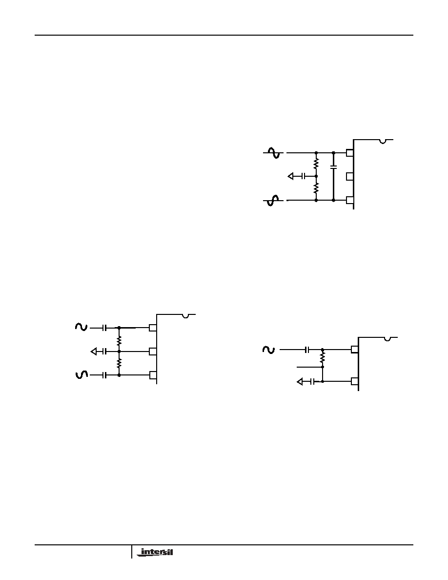
Analog Input, Differential Connection
The analog input to the HI5767 is a differential input that can
be configured in various ways depending on the signal
source and the required level of performance. A fully
differential connection (Figure 17 and Figure 18) will deliver
the best performance from the converter.
Since the HI5767 is powered by a single +5V analog supply,
the analog input is limited to be between ground and +5V.
For the differential input connection this implies the analog
input common mode voltage can range from 0.25V to 4.75V.
The performance of the ADC does not change significantly
with the value of the analog input common mode voltage.
A DC voltage source, VDC, equal to 3.2V (typical), is made
available to the user to help simplify circuit design when using
an AC coupled differential input. This low output impedance
voltage source is not designed to be a reference but makes
an excellent DC bias source and stays well within the analog
input common mode voltage range over temperature.
For the AC coupled differential input (Figure 17) and with
VREFIN connected to VREFOUT, full scale is achieved when
the VIN and -VIN input signals are 0.5VP-P , with -VIN being
180 degrees out of phase with VIN. The converter will be at
positive full scale when the VIN+ input is at VDC + 0.25V and
the VIN- input is at VDC - 0.25V (VIN+ - VIN- = +0.5V).
Conversely, the converter will be at negative full scale when
the VIN+ input is equal to VDC - 0.25V and VIN- is at
VDC + 0.25V (VIN+ - VIN- = -0.5V).
The analog input can be DC coupled (Figure 18) as long as
the inputs are within the analog input common mode voltage
range (0.25V
≤ VDC ≤ 4.75V).
The resistors, R, in Figure 18 are not absolutely necessary
but may be used as load setting resistors. A capacitor, C,
connected from VIN+ to VIN- will help filter any high
frequency noise on the inputs, also improving performance.
Values around 20pF are sufficient and can be used on AC
coupled inputs as well. Note, however, that the value of
capacitor C chosen must take into account the highest
frequency component of the analog input signal.
Analog Input, Single-Ended Connection
The configuration shown in Figure 19 may be used with a
single ended AC coupled input.
Again, with VREFIN connected to VREFOUT, if VIN is a 1VP-P
sinewave, then VIN+ is a 1.0VP-P sinewave riding on a positive
voltage equal to VDC. The converter will be at positive full scale
when VIN+ is at VDC + 0.5V (VIN+ - VIN- = +0.5V) and will be at
negative full scale when VIN+ is equal to VDC - 0.5V (VIN+ - VIN-
= -0.5V). Sufficient headroom must be provided such that the
input voltage never goes above +5V or below AGND. In this
case, VDC could range between 0.5V and 4.5V without a
significant change in ADC performance. The simplest way to
produce VDC is to use the DC bias source, VDC, output of the
HI5767.
VIN+
VDC
VIN-
HI5767
VIN
-VIN
R
FIGURE 16. AC COUPLED DIFFERENTIAL INPUT
VIN+
VDC
VIN-
HI5767
VIN
-VIN
R
C
VDC
FIGURE 17. DC COUPLED DIFFERENTIAL INPUT
VIN+
VIN-
HI5767
VIN
VDC
R
FIGURE 18. AC COUPLED SINGLE ENDED INPUT
HI5767
相关PDF资料 |
PDF描述 |
|---|---|
| MAX4952CTO+ | IC RE-DRIVER 4CH SAS/SATA 42TQFN |
| V375C12M150BL2 | CONVERTER MOD DC/DC 12V 150W |
| VI-243-MX-F2 | CONVERTER MOD DC/DC 24V 75W |
| HI5767/4CB | CONV A/D 10BIT 40MSPS 28-SOIC |
| VE-26D-IU-F1 | CONVERTER MOD DC/DC 85V 200W |
相关代理商/技术参数 |
参数描述 |
|---|---|
| HI5767EVAL1 | 功能描述:数据转换 IC 开发工具 HI5767 LW FREQUENCY EVALUATION PLATFORM RoHS:否 制造商:Texas Instruments 产品:Demonstration Kits 类型:ADC 工具用于评估:ADS130E08 接口类型:SPI 工作电源电压:- 6 V to + 6 V |
| HI5767EVAL2 | 功能描述:数据转换 IC 开发工具 HI5767 HI FREQUENCY EVALUATION PLATFORM RoHS:否 制造商:Texas Instruments 产品:Demonstration Kits 类型:ADC 工具用于评估:ADS130E08 接口类型:SPI 工作电源电压:- 6 V to + 6 V |
| HI5780 | 制造商:INTERSIL 制造商全称:Intersil Corporation 功能描述:10-Bit, 80 MSPS, High Speed, Low Power D/A Converter |
| HI5780-EV | 制造商:INTERSIL 制造商全称:Intersil Corporation 功能描述:10-Bit, 80 MSPS, High Speed, Low Power D/A Converter |
| HI5780JCQ | 制造商:Rochester Electronics LLC 功能描述:32 PQFP COMTEMP VIDEO D/A 10BIT 80MHZ - Bulk 制造商:Harris Corporation 功能描述: |
发布紧急采购,3分钟左右您将得到回复。