参数资料
| 型号: | HI5812KIB |
| 厂商: | Intersil |
| 文件页数: | 4/16页 |
| 文件大小: | 0K |
| 描述: | ADC 12BIT 50KSPS 1LSB 24-SOIC |
| 标准包装: | 30 |
| 位数: | 12 |
| 采样率(每秒): | 50k |
| 数据接口: | 并联 |
| 转换器数目: | 1 |
| 功率耗散(最大): | 25mW |
| 电压电源: | 模拟和数字 |
| 工作温度: | -40°C ~ 85°C |
| 安装类型: | 表面贴装 |
| 封装/外壳: | 24-SOIC(0.295",7.50mm 宽) |
| 供应商设备封装: | 24-SOIC |
| 包装: | 管件 |
| 输入数目和类型: | 1 个单端,单极 |
12
Depending on how long the clock was shut off, the low
portion of clock period 2 may be longer than during the
remaining cycles.
The input will continue to track until the end of period 3, the
same as when free running.
Figure 2 illustrates the same operation as above but with an
external clock. If STRT is removed (at least tRSTRT) before
clock period 2, a low signal applied to STRT will drop the
DRDY flag as before, and with the first positive-going clock
edge that meets the (tSUSTRT) setup time, the converter will
continue with clock period 3.
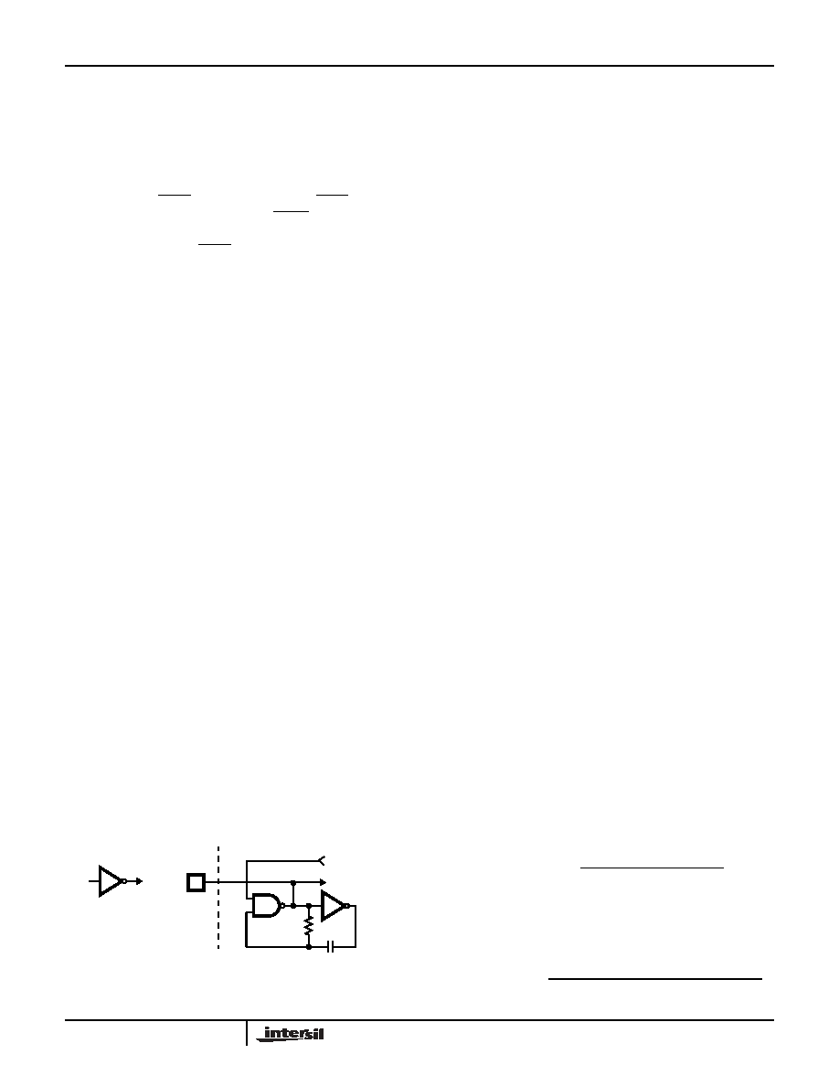
Clock
The HI5812 can operate either from its internal clock or from
one externally supplied. The CLK pin functions either as the
clock output or input. All converter functions are
synchronized with the rising edge of the clock signal.
Figure 21 shows the configuration of the internal clock. The
clock output drive is low power: if used as an output, it
should not have more than 1 CMOS gate load applied, and
stray wiring capacitance should be kept to a minimum.
The internal clock will shut down if the A/D is not restarted
after a conversion. The clock could also be shut down with
an open collector driver applied to the CLK pin. This should
only be done during the sample portion (the first three clock
periods) of a conversion cycle, and might be useful for using
the device as a digital sample and hold.
If an external clock is supplied to the CLK pin, it must have
sufficient drive to overcome the internal clock source. The
external clock can be shut off, but again, only during the
sample portion of a conversion cycle. At other times, it must
be above the minimum frequency shown in the
specifications. In the above two cases, a further restriction
applies in that the clock should not be shut off during the
third sample period for more than 1ms. This might cause an
internal charge-pump voltage to decay.
If the internal or external clock was shut off during the
conversion time (clock cycles 4 through 15) of the A/D, the
output might be invalid due to balancing capacitor droop.
An external clock must also meet the minimum tLOW and
tHIGH times shown in the specifications. A violation may
cause an internal miscount and invalidate the results.
Power Supplies and Grounding
VDD and VSS are the digital supply pins: they power all
internal logic and the output drivers. Because the output
drivers can cause fast current spikes in the VDD and VSS
lines, VSS should have a low impedance path to digital
ground and VDD should be well bypassed.
Except for VAA+, which is a substrate connection to VDD, all
pins have protection diodes connected to VDD and VSS.
Input transients above VDD or below VSS will get steered to
the digital supplies.
The VAA+ and VAA- terminals supply the charge-balancing
comparator only. Because the comparator is autobalanced
between conversions, it has good low-frequency supply
rejection. It does not reject well at high frequencies however;
VAA- should be returned to a clean analog ground and VAA+
should be RC decoupled from the digital supply as shown in
Figure 22.
There is approximately 50
of substrate impedance
between VDD and VAA+. This can be used, for example, as
part of a low-pass RC filter to attenuate switching supply
noise. A 10
F capacitor from VAA+ to ground would
attenuate 30kHz noise by approximately 40dB. Note that
back-to-back diodes should be placed from VDD to VAA+ to
handle supply to capacitor turn-on or turn-off current spikes.
Dynamic Performance
Fast Fourier Transform (FFT) techniques are used to
evaluate the dynamic performance of the A/D. A low
distortion sine wave is applied to the input of the A/D
converter. The input is sampled by the A/D and its output
stored in RAM. The data is than transformed into the
frequency domain with a 4096 point FFT and analyzed to
evaluate the converters dynamic performance such as SNR
and THD. See typical performance characteristics.
Signal-To-Noise Ratio
The signal to noise ratio (SNR) is the measured RMS signal
to RMS sum of noise at a specified input and sampling
frequency. The noise is the RMS sum of all except the
fundamental and the first five harmonic signals. The SNR is
dependent on the number of quantization levels used in the
converter. The theoretical SNR for an N-bit converter with no
differential or integral linearity error is: SNR = (6.02N + 1.76)
dB. For an ideal 12-bit converter the SNR is 74dB.
Differential and integral linearity errors will degrade SNR.
Signal-To-Noise + Distortion Ratio
SINAD is the measured RMS signal to RMS sum of noise
plus harmonic power and is expressed by the following:
OPTIONAL
CLK
INTERNAL
100k
18pF
CLOCK
ENABLE
EXTERNAL
CLOCK
FIGURE 21. INTERNAL CLOCK CIRCUITRY
SNR = 10 Log
Sinewave Signal Power
Total Noise Power
SINAD = 10 Log
Sinewave Signal Power
Noise + Harmonic Power (2nd - 6th)
HI5812
相关PDF资料 |
PDF描述 |
|---|---|
| MS27484T22A21SB | CONN PLUG 21POS STRAIGHT W/SCKT |
| MS27474E12F98P | CONN RCPT 10POS JAM NUT W/PINS |
| MS3106F32-1S | CONN PLUG 5POS STRAIGHT W/SCKT |
| D38999/26WH55PA | CONN PLUG 55POS STRAIGHT W/PINS |
| MS27505E15F5SC | CONN RCPT 5POS BOX MNT W/SCKT |
相关代理商/技术参数 |
参数描述 |
|---|---|
| HI5812KIBZ | 功能描述:ADC 12BIT 50KSPS 1LSB 24-SOIC RoHS:是 类别:集成电路 (IC) >> 数据采集 - 模数转换器 系列:- 产品培训模块:Lead (SnPb) Finish for COTS Obsolescence Mitigation Program 标准包装:2,500 系列:- 位数:12 采样率(每秒):3M 数据接口:- 转换器数目:- 功率耗散(最大):- 电压电源:- 工作温度:- 安装类型:表面贴装 封装/外壳:SOT-23-6 供应商设备封装:SOT-23-6 包装:带卷 (TR) 输入数目和类型:- |
| HI5812KIJ | 制造商:INTERSIL 制造商全称:Intersil Corporation 功能描述:CMOS 20 Microsecond, 12-Bit, Sampling A/D Converter with Internal Track and Hold |
| HI5812KIP | 制造商:INTERSIL 制造商全称:Intersil Corporation 功能描述:CMOS 20 Microsecond, 12-Bit, Sampling A/D Converter with Internal Track and Hold |
| HI5812KIPS2267 | 制造商:Harris Corporation 功能描述: 制造商:Intersil Corporation 功能描述: |
| HI5813 | 制造商:INTERSIL 制造商全称:Intersil Corporation 功能描述:CMOS 3.3V, 25 Microsecond, 12-Bit, Sampling A/D Converter with Internal Track and Hold |
发布紧急采购,3分钟左右您将得到回复。