参数资料
| 型号: | HI5828IN |
| 厂商: | Intersil |
| 文件页数: | 7/12页 |
| 文件大小: | 0K |
| 描述: | DAC DUAL 12BIT 130MHZ 48-LQFP |
| 标准包装: | 250 |
| 设置时间: | 35ns |
| 位数: | 12 |
| 数据接口: | 并联 |
| 转换器数目: | 2 |
| 电压电源: | 模拟和数字 |
| 功率耗散(最大): | 280mW |
| 工作温度: | -40°C ~ 85°C |
| 安装类型: | 表面贴装 |
| 封装/外壳: | 48-LQFP |
| 供应商设备封装: | 48-TQFP(7x7) |
| 包装: | 托盘 |
| 输出数目和类型: | 2 电流,单极 |
| 采样率(每秒): | 130M |
4
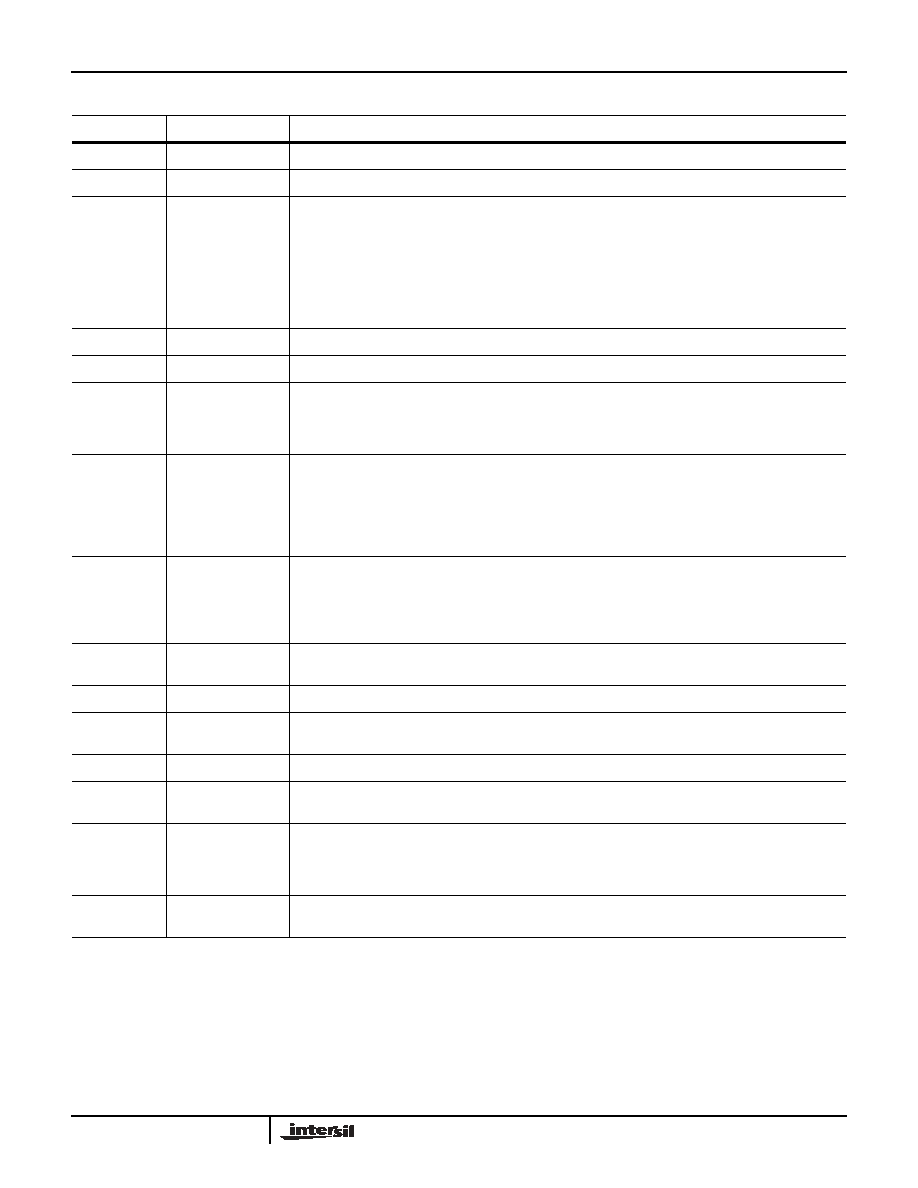
Pin Descriptions
PIN NO.
PIN NAME
PIN DESCRIPTION
11, 19, 26
AGND
Analog Ground.
13, 24
AVDD
Analog Supply (+2.7V to +5.5V).
28
CLK
Clock Input. The master and slave latches shown in the functional block diagram are simple D-latches.
Input data to the DAC passes through the “master” latches when the clock is low and is latched into the
“master” latches when the clock is high. Data presented to the “slave” latch passes through when the
clock is logic high and is latched into the “slave” latches when the clock is logic low. Adequate setup time
must be allowed for the MSBs to pass through the thermometer decoder before the clock goes high. This
master-slave arrangement comprises an edge-triggered flip-flop, with the DAC being updated on the
rising clock edge. It is recommended that the clock edge be skewed such that setup time is larger than
hold time for optimum spectral performance.
27
DGND
Connect to Digital Ground.
10
DVDD
Digital Supply (+2.7V to +5.5V).
20
FSADJ
Full Scale Current Adjust. Use a resistor to analog ground to adjust full scale output current. Full Scale
Output Current = 32 x VFSADJ/RSET. Where VFSADJ is the voltage at this pin. VFSADJ tracks the voltage
on the REFIO pin (refer to the functional block diagram); which is typically 1.2V if the internal reference
is used.
14, 23
ICOMP1, QCOMP1
Compensation Pin for Use in Reducing Bandwidth/Noise. Each pin should be individually decoupled to
AVDD with a 0.1
F capacitor. To minimize crosstalk, the part was designed so that these pins must be
connected externally, ideally directly under the device packaging. The voltage on these pins is used to
drive the gates of the PMOS devices that make up the current cells. Only the ICOMP1 pin is driven and
therefore QCOMP1 needs to be connected to ICOMP1, but de-coupled separately to minimize crosstalk.
If placed equally close to both pins, then only one decoupling capacitor might be necessary.
12, 25
ICOMP2, QCOMP2
Compensation Pin for Internal Bias Generation. Each pin should be individually decoupled to AGND with
a 0.1
F capacitor. The voltage generated at these pins represents the voltage used to supply power to
the switch drivers (refer to the functional block diagram) which is 2.0V nominal. This arrangement helps
to minimize clock feedthrough to the current cell transistors for reduced glitch energy and improved
spectral performance.
43-48, 1-6,
29-40
ID11-ID0, QD11-QD0 Digital Data Input Ports. Bit 11 is Most Significant Bit (MSB) and bit 0 is the Least Significant Bit (LSB).
15, 22
IOUTA, QOUTA
Current Outputs of the Device. Full scale output current is achieved when all input bits are set to binary 1.
16, 21
IOUTB, QOUTB
Complementary Current Outputs of the Device. Full scale output current is achieved on the
complementary outputs when all input bits are set to binary 0.
7, 8, 41, 42
N.C.
No Connection. Future LSBs for dual 14-bit DAC.
17
REFIO
Reference voltage input if Internal reference is disabled. The internal reference is not intended to drive an
external load. Use 0.1
F cap to ground when internal reference is enabled.
18
REFLO
Reference Low Select. When the internal reference is enabled, this pin serves as the precision ground
reference point for the internal voltage reference circuitry and therefore needs to have a good connection
to analog ground to enable internal 1.2V reference. To disable the internal reference circuitry this pin
should be connected to AVDD.
9
SLEEP
Control Pin for Power-Down Mode. Sleep Mode is active high; connect to ground for Normal Mode. The
Sleep pin has internal 25
A (nominal) active pulldown current.
HI5828
相关PDF资料 |
PDF描述 |
|---|---|
| HI5860IBZ | CONV D/A 12-BIT 130MSPS 28-SOIC |
| HI5960IAZ | CONV D/A 14BIT 130MSPS 28-TSSOP |
| HI7188IN | CONV A/D 16BIT 8:1 MUX 44-MQFP |
| HI7190IP | IC ADC 24BIT PROGBL SER 20-PDIP |
| HI7191IP | IC ADC 24BIT PROGBL SER 20-PDIP |
相关代理商/技术参数 |
参数描述 |
|---|---|
| HI5860 | 制造商:INTERSIL 制造商全称:Intersil Corporation 功能描述:12-Bit, 125MSPS, CommLinkTM High Speed D/A Converter |
| HI5860 WAF | 制造商:Intersil Corporation 功能描述: |
| HI5860_05 | 制造商:INTERSIL 制造商全称:Intersil Corporation 功能描述:12-Bit, 130MSPS, High Speed D/A Converter |
| HI5860_08 | 制造商:INTERSIL 制造商全称:Intersil Corporation 功能描述:12-Bit, 130MSPS, High Speed D/A Converter |
| HI5860IA | 功能描述:CONV D/A 12BIT 130MSPS 28-TSSOP RoHS:否 类别:集成电路 (IC) >> 数据采集 - 数模转换器 系列:- 标准包装:2,400 系列:- 设置时间:- 位数:18 数据接口:串行 转换器数目:3 电压电源:模拟和数字 功率耗散(最大):- 工作温度:-40°C ~ 85°C 安装类型:表面贴装 封装/外壳:36-TFBGA 供应商设备封装:36-TFBGA 包装:带卷 (TR) 输出数目和类型:* 采样率(每秒):* |
发布紧急采购,3分钟左右您将得到回复。