参数资料
| 型号: | HI7190IP |
| 厂商: | Intersil |
| 文件页数: | 9/25页 |
| 文件大小: | 0K |
| 描述: | IC ADC 24BIT PROGBL SER 20-PDIP |
| 标准包装: | 18 |
| 位数: | 24 |
| 数据接口: | 串行,SPI? |
| 转换器数目: | 1 |
| 功率耗散(最大): | 32.5mW |
| 电压电源: | 模拟和数字,双 ± |
| 工作温度: | -40°C ~ 85°C |
| 安装类型: | 通孔 |
| 封装/外壳: | 20-DIP(0.300",7.62mm) |
| 供应商设备封装: | 20-PDIP |
| 包装: | 管件 |
| 输入数目和类型: | 1 个差分,单极;1 个差分,双极 |
17
FN3612.10
June 27, 2006
DRDY - Data Ready. This is an output status flag from the
device to signal that the Data Output Register has been
updated with the new conversion result. DRDY is useful as an
edge or level sensitive interrupt signal to a microprocessor or
microcontroller. DRDY low indicates that new data is available
at the Data Output Register. DRDY will return high upon
completion of a complete Data Output Register read cycle.
MODE - Mode. This input is used to select between
Synchronous Self Clocking Mode (‘1’) or the Synchronous
External Clocking Mode (‘0’). When this pin is tied to VDD the
serial port is configured in the Synchronous Self Clocking
mode where the synchronous shift clock (SCLK) for the serial
port is generated by the HI7190 and has a frequency of
OSC1/8. When the pin is tied to DGND the serial port is
configured for the Synchronous External Clocking Mode
where the synchronous shift clock for the serial port is
generated by an external device up to a maximum frequency
of 5MHz.
Programming the Serial Interface
It is useful to think of the HI7190 interface in terms of
communication cycles. Each communication cycle happens
in 2 phases. The first phase of every communication cycle
is the writing of an instruction byte. The second phase is
the data transfer as described by the instruction byte. It is
important to note that phase 2 of the communication cycle
can be a single byte or a multi-byte transfer of data. For
example, the 3-byte Data Output Register can be read
using one multi-byte communication cycle rather than three
single-byte communication cycles. It is up to the user to
maintain synchronism with respect to data transfers. If the
system processor “gets lost” the only way to recover is to
and a 3-wire data transfer.
Several formats are available for reading from and writing to
the HI7190 registers in both the 2-wire and 3-wire protocols.
A portion of these formats is controlled by the CR<2:1> (BD
and MSB) bits which control the byte direction and bit order
of a data transfer respectively. These two bits can be written
in any combination but only the two most useful will be
discussed here.
The first combination is to reset both the BD and MSB bits
(BD = 0, MSB = 0). This sets up the interface for descending
byte order and MSB first format. When this combination is
used the user should always write the Instruction Register
such that the starting byte is the most significant byte
address. For example, read three bytes of DR starting with
the most significant byte. The first byte read will be the most
significant in MSB to LSB format. The next byte will be the
next least significant (recall descending byte order) again in
MSB to LSB order. The last byte will be the next lesser
significant byte in MSB to LSB order. The entire word was
read MSB to LSB format.
The second combination is to set both the BD and MSB bits
to 1. This sets up the interface for ascending byte order and
LSB first format. When this combination is used the user
should always write the Instruction Register such that the
starting byte is the least significant byte address. For
example, read three bytes of DR starting with the least
significant byte. The first byte read will be the least
significant in LSB to MSB format. The next byte will be the
next greater significant (recall ascending byte order) again in
LSB to MSB order. The last byte will be the next greater
significant byte in LSB to MSB order. The entire word was
read MSB to LSB format.
After completion of each communication cycle, The HI7190
interface enters a standby mode while waiting to receive a
new instruction byte.
Instruction Byte Phase
The instruction byte phase initiates a data transfer
sequence. The processor writes an 8-bit byte (Instruction
Byte) to the Instruction Register. The instruction byte informs
the HI7190 about the Data transfer phase activities and
includes the following information:
Read or Write cycle
Number of Bytes to be transferred
Which register and starting byte to be accessed
Data Transfer Phase
In the data transfer phase, data transfer takes place as set
by the Instruction Register contents. See Write Operation
and Read Operation sections for detailed descriptions.
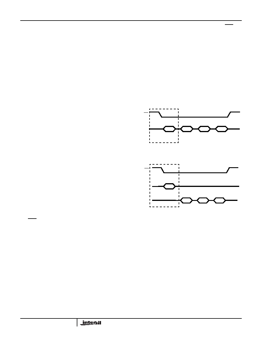
INSTRUCTION
BYTE
DATA
BYTE 1
DATA
BYTE 2
DATA
BYTE 3
INSTRUCTION
DATA TRANSFER
CYCLE
CS
SDIO
FIGURE 13A. 2-WIRE, 3-BYTE READ OR WRITE TRANSFER
INSTRUCTION
BYTE
DATA
BYTE 1
DATA
BYTE 2
DATA
BYTE 3
INSTRUCTION
DATA TRANSFER
CYCLE
CS
SDIO
SDO
FIGURE 13B. 3-WIRE, 3-BYTE READ TRANSFER
HI7190
相关PDF资料 |
PDF描述 |
|---|---|
| HI7191IP | IC ADC 24BIT PROGBL SER 20-PDIP |
| HI9P5701K-5 | CONV A/D 6BIT 30MSPS 18-SOIC |
| HMC700LP4E | IC FRACT-N PLL 16BIT 24QFN |
| HMC703LP4E | IC FRACT-N PLL W/SWEEPR 24QFN |
| HMC704LP4E | IC FRACT-N PLL 16BIT 24QFN |
相关代理商/技术参数 |
参数描述 |
|---|---|
| HI7190IPZ | 功能描述:模数转换器 - ADC W/ANNEAL ADC 24BIT 1 0HZ SIGMADELTA RoHS:否 制造商:Texas Instruments 通道数量:2 结构:Sigma-Delta 转换速率:125 SPs to 8 KSPs 分辨率:24 bit 输入类型:Differential 信噪比:107 dB 接口类型:SPI 工作电源电压:1.7 V to 3.6 V, 2.7 V to 5.25 V 最大工作温度:+ 85 C 安装风格:SMD/SMT 封装 / 箱体:VQFN-32 |
| HI7191 | 制造商:INTERSIL 制造商全称:Intersil Corporation 功能描述:24-Bit, High Precision, Sigma Delta A/D Converter |
| HI7191_06 | 制造商:INTERSIL 制造商全称:Intersil Corporation 功能描述:24-Bit, High Precision, Sigma Delta A/D Converter |
| HI7191IB | 功能描述:IC ADC 24BIT PROGBL SER 20-SOIC RoHS:否 类别:集成电路 (IC) >> 数据采集 - 模数转换器 系列:- 产品培训模块:Lead (SnPb) Finish for COTS Obsolescence Mitigation Program 标准包装:2,500 系列:- 位数:12 采样率(每秒):3M 数据接口:- 转换器数目:- 功率耗散(最大):- 电压电源:- 工作温度:- 安装类型:表面贴装 封装/外壳:SOT-23-6 供应商设备封装:SOT-23-6 包装:带卷 (TR) 输入数目和类型:- |
| HI7191IBZ | 功能描述:模数转换器 - ADC ADC 24BIT SIGMADELTA 20 IND RoHS:否 制造商:Texas Instruments 通道数量:2 结构:Sigma-Delta 转换速率:125 SPs to 8 KSPs 分辨率:24 bit 输入类型:Differential 信噪比:107 dB 接口类型:SPI 工作电源电压:1.7 V to 3.6 V, 2.7 V to 5.25 V 最大工作温度:+ 85 C 安装风格:SMD/SMT 封装 / 箱体:VQFN-32 |
发布紧急采购,3分钟左右您将得到回复。