参数资料
| 型号: | HI7191IBZ-T |
| 厂商: | Intersil |
| 文件页数: | 5/25页 |
| 文件大小: | 0K |
| 描述: | CONV A/D 24BIT SIGMA/DLTA 20SOIC |
| 产品培训模块: | Solutions for Industrial Control Applications |
| 标准包装: | 1 |
| 位数: | 24 |
| 数据接口: | 串行,SPI? |
| 转换器数目: | 1 |
| 功率耗散(最大): | 32.5mW |
| 电压电源: | 模拟和数字,双 ± |
| 工作温度: | -40°C ~ 85°C |
| 安装类型: | 表面贴装 |
| 封装/外壳: | 20-SOIC(0.295",7.50mm 宽) |
| 供应商设备封装: | 20-SOIC W |
| 包装: | 标准包装 |
| 输入数目和类型: | 1 个差分,单极;1 个差分,双极 |
| 其它名称: | HI7191IBZ-TDKR |
13
FN4138.8
June 1, 2006
notch code NOT the absolute frequency. The error is
seen when the user applies mid-scale (0V input, Bipolar
mode). With this input, the expected digital output
should be mid-scale (800000h). Instead, there is a small
probability, of an erroneous negative full scale (000000h)
output. Refer to Technical Brief TB348 for complete
details.
The FP10 to FP0 bits programmed into the Control Register
determine the cutoff (or notch) frequency of the digital filter.
The allowable code range is 00AH. This corresponds to a
maximum and minimum cutoff frequency of 1.953kHz and
10Hz, respectively when operating at a clock frequency of
10MHz. If a 1MHz clock is used then the maximum and
minimum cutoff frequencies become 195.3kHz and 1Hz,
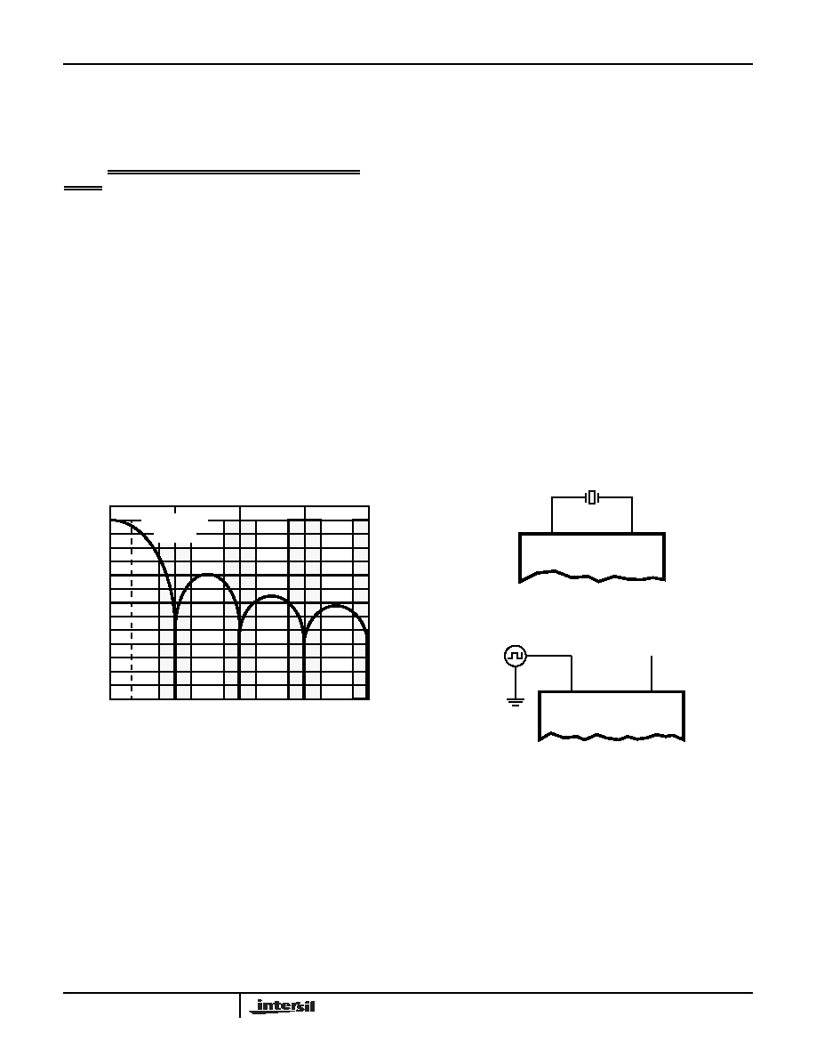
respectively. A plot of the (sinx/x)3 digital filter characteristics
is shown in Figure 10. This filter provides greater than 120dB
of 50Hz or 60Hz rejection. Changing the clock frequency or
the programming of the FP bits does not change the shape
of the filter characteristics, it merely shifts the notch
frequency. This low pass digital filter at the output of the
converter has an accompanying settling time for step inputs
just as a low pass analog filter does. New data takes
between 3 and 4 conversion periods to settle and update on
the serial port with a conversion period tCONV being equal to
1/fN.
Input Filtering
The digital filter does not provide rejection at integer
multiples of the modulator sampling frequency. This implies
that there are frequency bands where noise passes to the
output without attenuation. For most cases this is not a
problem because the high oversampling rate and noise
shaping characteristics of the modulator cause this noise to
become a small portion of the broadband noise which is
filtered. However, if an anti-alias filter is necessary a single
pole RC filter is usually sufficient.
If an input filter is used the user must be careful that the
source impedance of the filter is low enough not to cause
gain errors in the system. The DC input impedance at the
inputs is >1G
Ω but it is a dynamic load that changes with
clock frequency and selected gain. The input sample rate,
also dependent upon clock frequency and gain, determines
the allotted time for the input capacitor to charge. The
addition of external components may cause the charge time
of the capacitor to increase beyond the allotted time. The
result of the input not settling to the proper value is a system
gain error which can be eliminated by system calibration of
the HI7191.
Clocking/Oscillators
The master clock into the HI7191 can be supplied by either a
crystal connected between the OSC1 and OSC2 pins as
shown in Figure 10A or a CMOS compatible clock signal
connected to the OSC1 pin as shown in Figure 10B. The
input sampling frequency, modulator sampling frequency,
filter -3dB frequency, output update rate, and calibration time
are all directly related to the master clock frequency, fOSC.
For example, if a 1MHz clock is used instead of a 10MHz
clock, what is normally a 10Hz conversion rate becomes a
1Hz conversion rate. Lowering the clock frequency will also
lower the amount of current drawn from the power supplies.
Please note that the HI7191 specifications are written for a
10MHz clock only.
Operational Modes
The HI7191 contains several operational modes including
calibration modes for cancelling offset and gain errors of
both internal and external circuitry. A calibration routine
should be initiated whenever there is a change in the
ambient operating temperature or supply voltage. Calibration
should also be initiated if there is a change in the gain, filter
notch, bipolar, or unipolar input range. Non-calibrated data
can be obtained from the device by writing 000000 to the
Offset Calibration Register, 800000 (h) to the Positive Full
ALIAS BAND
fN ±fC
FREQUENCY (Hz)
AMPLITUDE
(dB)
fN
fC
2fN
3fN
4fN
0
-20
-40
-60
-80
-100
-120
FIGURE 9. LOW PASS FILTER FREQUENCY CHARACTERISTICS
FIGURE 10A.
FIGURE 10B.
FIGURE 10. OSCILLATOR CONFIGURATIONS
HI7191
OSC1
OSC2
10MHz
16
17
HI7191
OSC1
OSC2
10MHz
16
17
NO
CONNECTION
HI7191
相关PDF资料 |
PDF描述 |
|---|---|
| VI-211-MX-F3 | CONVERTER MOD DC/DC 12V 75W |
| IDT72V851L15PFI | IC FIFO SYNC 4096X18 15NS 64QFP |
| MAX11629EEE+ | ADC 12BIT 300KSPS 8CH 16-QSOP |
| MAX11200EEE+T | ADC 24BIT 1CH ULP GPIO 16-QSOP |
| IDT72V851L10PFG | IC FIFO SYNC 4096X18 10NS 64QFP |
相关代理商/技术参数 |
参数描述 |
|---|---|
| HI7191IP | 功能描述:IC ADC 24BIT PROGBL SER 20-PDIP RoHS:否 类别:集成电路 (IC) >> 数据采集 - 模数转换器 系列:- 产品培训模块:Lead (SnPb) Finish for COTS Obsolescence Mitigation Program 标准包装:2,500 系列:- 位数:12 采样率(每秒):3M 数据接口:- 转换器数目:- 功率耗散(最大):- 电压电源:- 工作温度:- 安装类型:表面贴装 封装/外壳:SOT-23-6 供应商设备封装:SOT-23-6 包装:带卷 (TR) 输入数目和类型:- |
| HI7191IPZ | 功能描述:模数转换器 - ADC W/ANNEAL ADC 24BIT SIGMADELTA 20PDIP RoHS:否 制造商:Texas Instruments 通道数量:2 结构:Sigma-Delta 转换速率:125 SPs to 8 KSPs 分辨率:24 bit 输入类型:Differential 信噪比:107 dB 接口类型:SPI 工作电源电压:1.7 V to 3.6 V, 2.7 V to 5.25 V 最大工作温度:+ 85 C 安装风格:SMD/SMT 封装 / 箱体:VQFN-32 |
| HI73127 | 制造商:Hanna 功能描述:Bulk |
| HI-73127 | 制造商:HANNA INSTRUMENTS 功能描述:ELECTRODE SPARE 制造商:HANNA INSTRUMENTS 功能描述:ELECTRODE, SPARE 制造商:HANNA INSTRUMENTS 功能描述:ELECTRODE, SPARE; pH Measuring Ranges:- |
| HI765PWL | 制造商:Hanna 功能描述: |
发布紧急采购,3分钟左右您将得到回复。