- 您现在的位置:买卖IC网 > Datasheet目录327 > HIP4020IBZ (Intersil)IC DRIVER FULL-BRIDGE 20-SOIC Datasheet资料下载
参数资料
| 型号: | HIP4020IBZ |
| 厂商: | Intersil |
| 文件页数: | 3/9页 |
| 文件大小: | 0K |
| 描述: | IC DRIVER FULL-BRIDGE 20-SOIC |
| 标准包装: | 38 |
| 配置: | 半桥 |
| 输入类型: | 反相和非反相 |
| 延迟时间: | 2.5µs |
| 电流 - 峰: | 625mA |
| 配置数: | 1 |
| 输出数: | 4 |
| 电源电压: | 3 V ~ 12 V |
| 工作温度: | -40°C ~ 85°C |
| 安装类型: | 表面贴装 |
| 封装/外壳: | 20-SOIC(0.295",7.50mm 宽) |
| 供应商设备封装: | 20-SOIC W |
| 包装: | 管件 |
| 产品目录页面: | 1239 (CN2011-ZH PDF) |
�� �
�
�HIP4020�
�Absolute� Maximum� Ratings�
�Supply� Voltage;� V� DD� to� V� SS� or� V� SSA� or� V� SSB� .� .� .� .� .� .� .� .� .� .� .� .� .+15V�
�Neg.� Output� Supply� Voltage,� (V� SSA� ,� V� SSB� )� .� .� .� .� .� .� .� .� .� .� .� .� (Note� 1)�
�DC� Logic� Input� Voltage� (Each� Input)� .� .� .� (V� SS� -0.5V)� to� (V� DD� +0.5V)�
�DC� Logic� Input� Current� (Each� Input)� .� .� .� .� .� .� .� .� .� .� .� .� .� .� .� .� .� .� .� .� .� ±� 15mA�
�ILF� Fault� Output� Current� .� .� .� .� .� .� .� .� .� .� .� .� .� .� .� .� .� .� .� .� .� .� .� .� .� .� .� .� .� .� .� .� ±� 15mA�
�Output� Load� Current,� (Self� Limiting,� See� Elec.� Spec.)� .� .� .� .� ±� I� O(LIMIT)�
�Thermal� Information�
�Thermal� Resistance� (Typical,� Note� 2)� θ� JA� (°C/W)�
�Plastic� SOIC� Package� .� .� .� .� .� .� .� .� .� .� .� .� .� .� .� .� .� .� .� .� .� .� .� 105�
�Maximum� Storage� Temperature� Range� .� .� .� .� .� .� .� .� .� .� .� -65°C� to� 150°C�
�Maximum� Junction� Temperature� .� .� .� .� .� .� .� .� .� .� .� .� .� .� .� .� .� .� .� .� .� .� .� 150°C�
�Maximum� Lead� Temperature� (Soldering� 10s)� .� .� .� .� .� .� .� .� .� .� .� .� .� 300°C�
�(Lead� Tips� Only)�
�Operating� Conditions� T� A� =� 25°C�
�Typical� Operating� Supply� Voltage� Range,� V� DD� .� .� .� .� .� .� .� +3� to� +12V�
�Low� Voltage� Logic� Retention,� Min.� V� DD� .� .� .� .� .� .� .� .� .� .� .� .� .� .� .� .� .� .� .� .+2V�
�Idle� Supply� Current;� No� Load,� V� DD� =� +5V.� .� .� .� .� .� .� .� .� .� .� .� .� .� .� .0.8mA�
�Typical� P+N� Channel� r� DS(ON)� ,� V� DD� =� +5V,� 0.5A� Load� .� .� .� .� .� .� .� .� 2� ?�
�CAUTION:� Stresses� above� those� listed� in� “Absolute� Maximum� Ratings”� may� cause� permanent� damage� to� the� device.� This� is� a� stress� only� rating� and� operation� of� the�
�device� at� these� or� any� other� conditions� above� those� indicated� in� the� operational� sections� of� this� specification� is� not� implied.�
�NOTES:�
�1.� V� SS� is� the� required� common� ground� reference� for� the� logic� input� switching.� The� load� currents� may� be� switched� positive� and� negative� in� reference�
�to� the� V� SS� common� ground� by� using� a� split� supply� for� V� DD� (positive)� to� V� SSA� and� V� SSB� (negative).� For� an� uneven� split� in� the� supply� voltage,�
�the� Maximum� Negative� Output� Supply� Voltage� for� V� SSA� and� V� SSB� is� limited� by� the� Maximum� V� DD� to� V� SSA� or� V� SSB� ratings.� Since� the� V� DD� pins�
�are� internally� tied� together,� the� voltage� on� each� V� DD� pins� must� be� equal� and� common.�
�2.� θ� JA� is� measured� with� the� component� mounted� on� an� evaluation� PC� board� in� free� air.�
�3.� Refer� to� the� Truth� Table� and� the� V� EN� to� V� OUT� Switching� Waveforms.� Current,� I� O� refers� to� I� OUTA� or� I� OUTB� as� the� Output� Load� current.� Note� that�
�ENA� controls� OUTA� and� ENB� controls� OUTB.� Each� Half� H-Switch� has� independent� control� from� the� respective� A1,� A2,� ENA� or� B1,� B2,� ENB�
�inputs.� Refer� to� the� Terminal� Information� Table� for� external� pin� connections� to� establish� mode� control� switching.� Figure� 1� shows� a� typical�
�application� circuit� used� to� control� a� DC� Motor.�
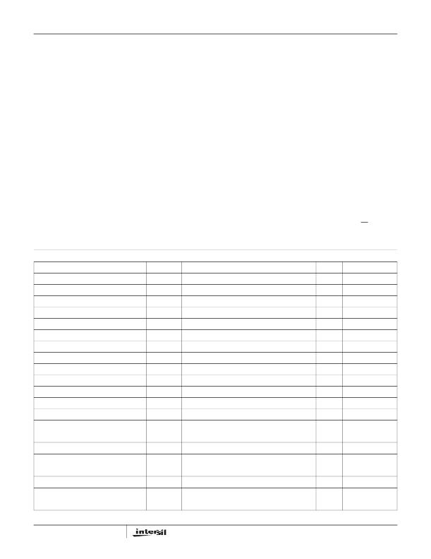
�Electrical� Specifications�
�T� A� =� 25°C,� V� DD� =� +5V,� V� SSA� =� V� SSB� =� V� SS� =� 0V,� Unless� Otherwise� Specified�
�PARAMETER�
�Input� Leakage� Current�
�Low� Level� Input� Voltage�
�High� Level� Input� Voltage�
�ILF� Output� Low,� Sink� Current�
�ILF� Output� High,� Source� Current�
�Input� Capacitance�
�P-Channel� rDS(ON),� Low� Supply� Voltage�
�N-Channel� rDS(ON),� Low� Supply� Voltage�
�P-Channel� rDS(ON),� High� Supply� Voltage�
�N-Channel� rDS(ON),� High� Supply� Voltage�
�OUTA,� OUTB� Source� Current� Limiting�
�OUTA,� OUTB� Sink� Current� Limiting�
�Idle� Supply� Current;� No� Load�
�OUTA,� OUTB� Voltage� High�
�OUTA,� OUTB� Voltage� Low�
�OUTA,� OUTB� Voltage� High�
�OUTA,� OUTB� Voltage� Low�
�OUTA,� OUTB� Source� Current� Limiting�
�OUTA,� OUTB� Sink� Current� Limiting�
�OUTA,� OUTB� Source� Current� Limiting�
�OUTA,� OUTB� Sink� Current� Limiting�
�SYMBOL�
�I� LEAK�
�V� IL�
�V� IH�
�I� OH�
�I� OL�
�C� IN�
�rDS(ON)�
�rDS(ON)�
�rDS(ON)�
�rDS(ON)�
�I� O(LIMIT)�
�-I� O(LIMIT)�
�I� DD�
�V� OH�
�V� OL�
�V� OH�
�V� OL�
�I� O(LIMIT)�
�-I� O(LIMIT)�
�I� O(LIMIT)�
�-I� O(LIMIT)�
�TEST� CONDITIONS�
�V� DD� =� +15V�
�V� OUT� =� 0.4V,� V� DD� =� +12V�
�V� OUT� =� 11.6V,� V� DD� =� +12V�
�V� DD� =� +3V,� I� SOURCE� =� 250mA�
�V� DD� =� +3V,� I� SINK� =� 250mA�
�V� DD� =� +12V,� I� SOURCE� =� 400mA�
�V� DD� =� +12V,� I� SINK� =� 400mA�
�V� DD� =� +6V,� V� SS� =� 0V,� V� SSA� =� V� SS� B� =� -6V�
�V� DD� =� +6V,� V� SS� =� 0V,� V� SSA� =� V� SS� B� =� -6V�
�I� SOURCE� =� 450mA�
�I� SINK� =� 450mA�
�V� DD� =� +3V,� I� SOURCE� =� 250mA�
�V� DD� =� +3V,� I� SINK� =� 250mA�
�V� DD� =� +12V�
�V� DD� =� +12V�
�V� DD� =� +3V�
�V� DD� =� +3V�
�MIN�
�-�
�V� SS�
�2�
�15�
�-�
�-�
�-�
�-�
�-�
�-�
�480�
�480�
�-�
�4.2�
�-�
�2.415�
�-�
�480�
�480�
�480�
�480�
�TYP�
�-�
�-�
�-�
�-�
�-�
�2�
�1.6�
�1�
�0.6�
�0.5�
�625�
�800�
�0.8�
�4.5�
�0.4�
�2.6�
�0.25�
�625�
�800�
�625�
�800�
�MAX�
�25�
�0.8�
�V� DD�
�-�
�-15�
�-�
�2.1�
�1.5�
�1.2�
�1.1�
�1500�
�1500�
�1.5�
�-�
�0.6�
�-�
�0.375�
�1500�
�1500�
�1500�
�1500�
�UNITS�
�nA�
�V�
�V�
�mA�
�mA�
�pF�
�?�
�?�
�?�
�?�
�mA�
�mA�
�mA�
�V�
�V�
�V�
�V�
�mA�
�mA�
�mA�
�mA�
�3�
�FN3976.3�
�December� 20,� 2005�
�相关PDF资料 |
PDF描述 |
|---|---|
| HIP4081AIP | IC DRIVER FULL-BRIDGE 20-DIP |
| HIP4082IP | IC DRIVER H-BRIDGE 16-DIP |
| HIP6004EVAL3 | EVALUATION BOARD EMBED HIP6004 |
| HIP6019BEVAL1 | EVAL BOARD 1 FOR HIP6019B |
| HIP6021EVAL1 | EVALUATION BOARD HIP6021 |
相关代理商/技术参数 |
参数描述 |
|---|---|
| HIP4020IBZT | 功能描述:马达/运动/点火控制器和驱动器 W/ANNEAL FL BRDG MOTOR DRVR/CNTRLR RoHS:否 制造商:STMicroelectronics 产品:Stepper Motor Controllers / Drivers 类型:2 Phase Stepper Motor Driver 工作电源电压:8 V to 45 V 电源电流:0.5 mA 工作温度:- 25 C to + 125 C 安装风格:SMD/SMT 封装 / 箱体:HTSSOP-28 封装:Tube |
| HIP4080 | 制造商:INTERSIL 制造商全称:Intersil Corporation 功能描述:80V/2.5A Peak, High Frequency Full Bridge FET Driver |
| HIP4080_03 | 制造商:INTERSIL 制造商全称:Intersil Corporation 功能描述:80V/2.5A Peak, High Frequency Full Bridge FET Driver |
| HIP4080A | 制造商:INTERSIL 制造商全称:Intersil Corporation 功能描述:80V/2.5A Peak, High Frequency Full Bridge FET Driver |
| HIP4080A/81AEVALZ | 功能描述:电源管理IC开发工具 HIP4080A/81A EVAL ION BRD ROHS CMPLNT RoHS:否 制造商:Maxim Integrated 产品:Evaluation Kits 类型:Battery Management 工具用于评估:MAX17710GB 输入电压: 输出电压:1.8 V |
发布紧急采购,3分钟左右您将得到回复。