- 您现在的位置:买卖IC网 > PDF目录385382 > HIP6016 (Intersil Corporation) FPGA - 100000 SYSTEM GATE 2.5 VOLT - NOT RECOMMENDED for NEW DESIGN PDF资料下载
参数资料
| 型号: | HIP6016 |
| 厂商: | Intersil Corporation |
| 元件分类: | FPGA |
| 英文描述: | FPGA - 100000 SYSTEM GATE 2.5 VOLT - NOT RECOMMENDED for NEW DESIGN |
| 中文描述: | 先进的双PWM和线性功率控制 |
| 文件页数: | 13/14页 |
| 文件大小: | 130K |
| 代理商: | HIP6016 |
2-208
placed very close to the upper MOSFET to suppress the
voltage induced in the parasitic circuit impedances.
For a through hole design, several electrolytic capacitors
(Panasonic HFQ series or Nichicon PL series or Sanyo MV-
GX or equivalent) may be needed. For surface mount designs,
solid tantalum capacitors can be used, but caution must be
exercised with regard to the capacitor surge current rating.
These capacitors must be capable of handling the surge-
current at power-up. The TPS series available from AVX, and
the 593D series from Sprague are both surge current tested.
MOSFET Selection/Considerations
The HIP6016 requires 3 N-Channel power MOSFETs. Two
MOSFETs are used in the synchronous-rectified buck
topology of the PWM converter. The linear controller drives a
MOSFET as a pass transistor. These should be selected
based upon r
DS(ON)
, gate supply requirements, and thermal
management requirements.
PWM MOSFET Selection and Considerations
In high-current PWM applications, the MOSFET power
dissipation, package selection and heatsink are the dominant
design factors. The power dissipation includes two loss
components; conduction loss and switching loss. These
losses are distributed between the upper and lower
MOSFETs according to duty factor (see the equations below).
The conduction loss is the only component of power
dissipation for the lower MOSFET. Only the upper MOSFET
has switching losses, since the lower device turns on into near
zero voltage.
The equations below assume linear voltage-current
transitions and do not model power loss due to the reverse-
recovery of the lower MOSFETs’ body diode. The
gate-charge losses are proportional to the switching
frequency (F
S
) and are dissipated by the HIP6016, thus not
contributing to the MOSFETs’ temperature rise. However,
large gate charge increases the switching interval, t
SW
which increases the upper MOSFET switching losses.
Ensure that both MOSFETs are within their maximum
junction temperature at high ambient temperature by
calculating the temperature rise according to package
thermal resistance specifications. A separate heatsink may
be necessary depending upon MOSFET power, package
type, ambient temperature and air flow.
The r
DS(ON)
is different for the two previous equations even
if the type device is used for both. This is because the gate
drive applied to the upper MOSFET is different than the
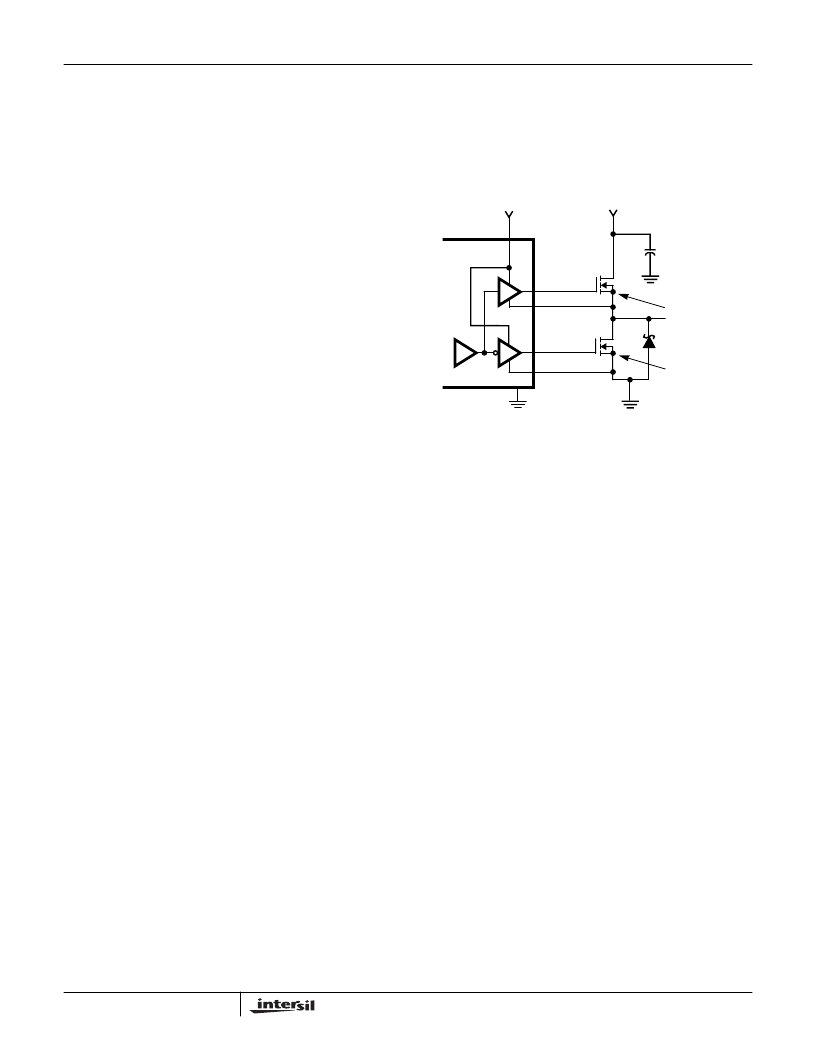
lower MOSFET. Figure 14 shows the gate drive where the
upper gate-to-source voltage is approximately V
CC
less the
input supply. For +5V main power and +12VDC for the bias,
the gate-to-source voltage of Q1 is 7V. The lower gate drive
voltage is +12VDC. A logic-level MOSFET is a good choice for
Q1 and a logic-level MOSFET can be used for Q2 if its
absolute gate-to-source voltage rating exceeds the maximum
voltage applied to V
CC
.
Rectifier CR1 is a clamp that catches the negative inductor
voltage swing during the dead time between the turn off of
the lower MOSFET and the turn on of the upper MOSFET.
The diode must be a Schottky type to prevent the lossy
parasitic MOSFET body diode from conducting. It is
acceptable to omit the diode and let the body diode of the
lower MOSFET clamp the negative inductor swing, but
efficiency might drop one or two percent as a result. The
diode’s rated reverse breakdown voltage must be greater
than twice the maximum input voltage.
Linear Controller MOSFET Selection
The main criteria for selection of a MOSFET for the linear
regulator is package selection for efficient removal of heat.
The power dissipated in a linear regulator is:
Select a package and heatsink that maintains the junction
temperature below the maximum rating while operating at
the highest expected ambient temperature.
PUPPER
IO
2
rDS ON
VIN
)
×
VOUT
×
IO
VIN
×
tSW
×
2
FS
×
+
=
PLOWER
IO
2
rDS ON
)
×
VIN
VOUT
–
(
)
×
VIN
=
+12V
PGND
HIP6016
GND
LGATE
UGATE
PHASE
VCC
+5V OR LESS
NOTE:
V
GS
≈
V
CC
-5V
NOTE:
V
GS
≈
V
CC
Q1
Q2
+
-
FIGURE 14. OUTPUT GATE DRIVERS
CR1
PLINEAR
IO
VIN
VOUT
–
(
)
×
=
HIP6016
相关PDF资料 |
PDF描述 |
|---|---|
| HIP6016CB | Advanced PWM and Dual Linear Power Control |
| HIP6017B | FPGA - 100000 SYSTEM GATE 2.5 VOLT - NOT RECOMMENDED for NEW DESIGN |
| HIP6017BCB | FPGA - 100000 SYSTEM GATE 2.5 VOLT - NOT RECOMMENDED for NEW DESIGN |
| HIP6018B | 100,000 System Gate FPGA - NOT RECOMMENDED for NEW DESIGN |
| HIP6018BCB | FPGA - 100000 SYSTEM GATE 2.5 VOLT - NOT RECOMMENDED for NEW DESIGN |
相关代理商/技术参数 |
参数描述 |
|---|---|
| HIP6016 WAF | 制造商:Intersil Corporation 功能描述: |
| HIP6016CB | 制造商:Rochester Electronics LLC 功能描述:- Bulk |
| HIP6016CB WAF | 制造商:Harris Corporation 功能描述: |
| HIP6016CB-T | 制造商:Rochester Electronics LLC 功能描述:ADVANCED PWM & CONTROL "3 IN 1"& 1.5V OUTPUTS T&R - Bulk |
| HIP6017 | 制造商:INTERSIL 制造商全称:Intersil Corporation 功能描述:Advanced PWM and Dual Linear Power Control |
发布紧急采购,3分钟左右您将得到回复。