- 您现在的位置:买卖IC网 > PDF目录385382 > HIP6017BCB (INTERSIL CORP) FPGA - 100000 SYSTEM GATE 2.5 VOLT - NOT RECOMMENDED for NEW DESIGN PDF资料下载
参数资料
| 型号: | HIP6017BCB |
| 厂商: | INTERSIL CORP |
| 元件分类: | 稳压器 |
| 英文描述: | FPGA - 100000 SYSTEM GATE 2.5 VOLT - NOT RECOMMENDED for NEW DESIGN |
| 中文描述: | SWITCHING CONTROLLER, 215 kHz SWITCHING FREQ-MAX, PDSO28 |
| 封装: | PLASTIC, MS-013AE, SOIC-28 |
| 文件页数: | 10/16页 |
| 文件大小: | 139K |
| 代理商: | HIP6017BCB |
10
Layout Considerations
MOSFETs switch very fast and efficiently. The speed with
which the current transitions from one device to another
causes voltage spikes across the interconnecting
impedances and parasitic circuit elements. The voltage
spikes can degrade efficiency, radiate noise into the circuit,
and lead to device over-voltage stress. Careful component
layout and printed circuit design minimizes the voltage
spikes in the converter. Consider, as an example, the turnoff
transition of the upper PWM MOSFET. Prior to turnoff, the
upper MOSFET was carrying the full load current. During the
turnoff, current stops flowing in the upper MOSFET and is
picked up by the lower MOSFET (and/or parallel Schottky
diode). Any inductance in the switched current path generates
a large voltage spike during the switching interval. Careful
component selection, tight layout of the critical components,
andshort,widecircuittracesminimizethemagnitudeofvoltage
spikes. Contact Intersil for evaluation board drawings of the
component placement and printed circuit board.
There are two sets of critical components in a DC-DC
converter using a HIP6017B controller. The power
components are the most critical because they switch large
amounts of energy. The critical small signal components
connect to sensitive nodes or supply critical bypassing
current.
The power components should be placed first. Locate the
input capacitors close to the power switches. Minimize the
length of the connections between the input capacitors and
the power switches. Locate the output inductor and output
capacitors between the MOSFETs and the load. Locate the
PWM controller close to the MOSFETs.
The critical small signal components include the bypass
capacitor for VCC and the soft-start capacitor, C
SS
. Locate
these components close to their connecting pins on the
control IC. Minimize any leakage current paths from SS node
because the internal current source is only 11
μ
A.
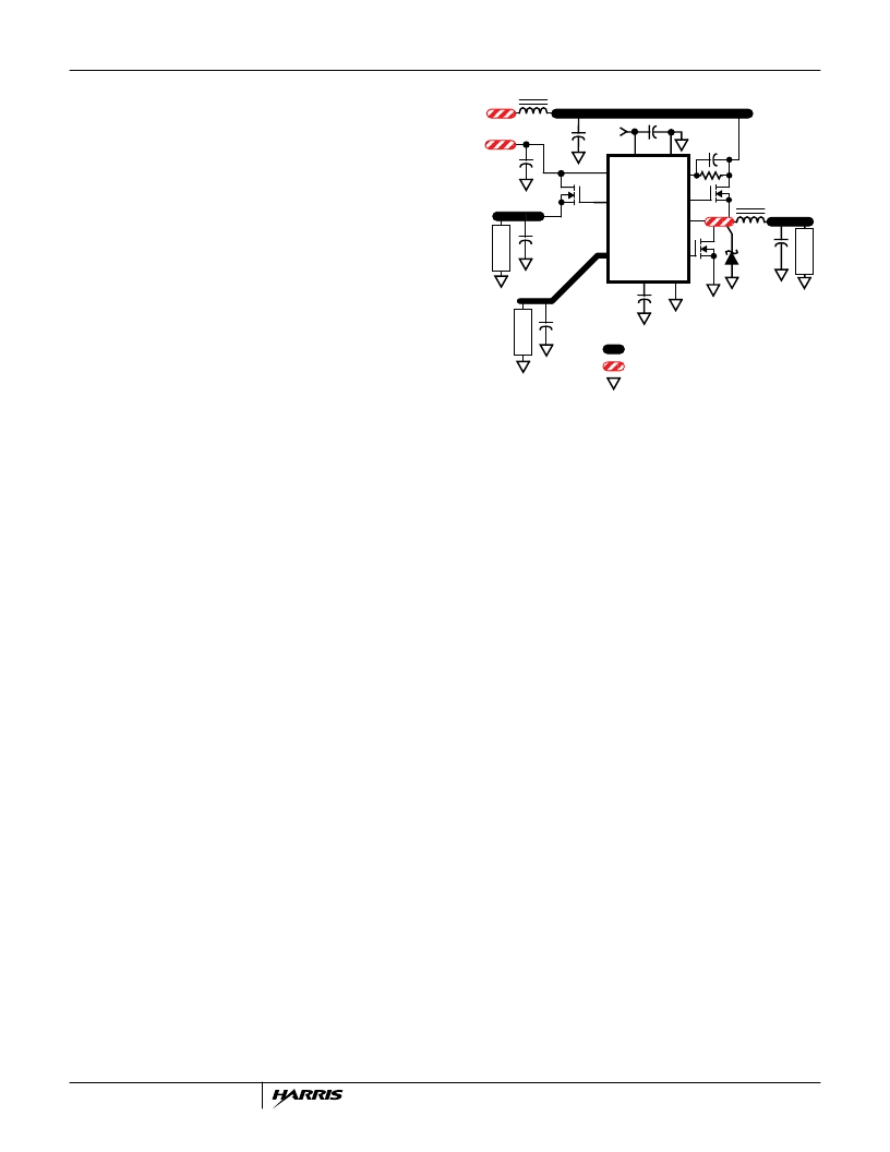
A multi-layer printed circuit board is recommended.
Figure 10 shows the connections of the critical components
in the converter. Note that capacitors C
IN
and C
OUT
could
each represent numerous physical capacitors. Dedicate one
solid layer for a ground plane and make all critical
component ground connections with vias to this layer.
Dedicate another solid layer as a power plane and break this
plane into smaller islands of common voltage levels. The
power plane should support the input power and output
power nodes. Use copper filled polygons on the top and
bottom circuit layers for the phase nodes. Use the remaining
printed circuit layers for small signal wiring. The wiring traces
from the control IC to the MOSFET gate and source should
be sized to carry 1A currents. The traces for OUT2 need only
be sized for 0.2A. Locate C
OUT2
close to the HIP6017B IC.
PWM Controller Feedback Compensation
Both PWM controllers use voltage-mode control for output
regulation. This section highlights the design consideration
for a voltage-mode controller. Apply the methods and
considerations to both PWM controllers.
Figure 11 highlights the voltage-mode control loop for a
synchronous-rectified buck converter. The output voltage is
regulated to the reference voltage level. The reference
voltage level is the DAC output voltage for the PWM
controller. The error amplifier output (V
E/A
) is compared with
the oscillator (OSC) triangular wave to provide a pulse-width
modulated wave with an amplitude of V
IN
at the PHASE
node. The PWM wave is smoothed by the output filter (L
O
and C
O
).
The modulator transfer function is the small-signal transfer
function of V
OUT
/V
E/A
. This function is dominated by a DC
gain and the output filter, with a double pole break frequency
at F
LC
and a zero at F
ESR
. The DC gain of the modulator is
simply the input voltage, V
IN
, divided by the peak-to-peak
oscillator voltage,
V
OSC
.
V
OUT1
Q1
Q2
C
SS
+12V
C
VCC
L
VIA CONNECTION TO GROUND PLANE
ISLAND ON POWER PLANE LAYER
ISLAND ON CIRCUIT PLANE LAYER
L
OUT1
C
OUT1
CR1
L
C
IN
V
OUT3
+5V
IN
FIGURE 10. PRINTED CIRCUIT BOARD POWER PLANES AND
ISLANDS
KEY
+3.3V
IN
Q3
L
C
OUT2
V
OUT2
R
OCSET1
C
OCSET1
HIP6018
SS PGND
LGATE1
UGATE1
PHASE1
DRIVE3
VCC
VIN2
GND
OCSET1
VOUT2
HIP6017B
相关PDF资料 |
PDF描述 |
|---|---|
| HIP6018B | 100,000 System Gate FPGA - NOT RECOMMENDED for NEW DESIGN |
| HIP6018BCB | FPGA - 100000 SYSTEM GATE 2.5 VOLT - NOT RECOMMENDED for NEW DESIGN |
| HIP6019 | FPGA - 100000 SYSTEM GATE 2.5 VOLT - NOT RECOMMENDED for NEW DESIGN |
| HIP6019CB | Advanced Dual PWM and Dual Linear Power Control |
| HIP6019EVAL1 | Advanced Dual PWM and Dual Linear Power Control |
相关代理商/技术参数 |
参数描述 |
|---|---|
| HIP6017BCB WAF | 制造商:Harris Corporation 功能描述: |
| HIP6017BCB-T | 制造商:Rochester Electronics LLC 功能描述:- Tape and Reel |
| HIP6017CB | 制造商:Rochester Electronics LLC 功能描述:- Bulk |
| HIP6017CB WAF | 制造商:Harris Corporation 功能描述: |
| HIP6017CB-T | 制造商:Rochester Electronics LLC 功能描述:- Bulk |
发布紧急采购,3分钟左右您将得到回复。