- 您现在的位置:买卖IC网 > PDF目录385382 > HIP6017BCB (INTERSIL CORP) FPGA - 100000 SYSTEM GATE 2.5 VOLT - NOT RECOMMENDED for NEW DESIGN PDF资料下载
参数资料
| 型号: | HIP6017BCB |
| 厂商: | INTERSIL CORP |
| 元件分类: | 稳压器 |
| 英文描述: | FPGA - 100000 SYSTEM GATE 2.5 VOLT - NOT RECOMMENDED for NEW DESIGN |
| 中文描述: | SWITCHING CONTROLLER, 215 kHz SWITCHING FREQ-MAX, PDSO28 |
| 封装: | PLASTIC, MS-013AE, SOIC-28 |
| 文件页数: | 11/16页 |
| 文件大小: | 139K |
| 代理商: | HIP6017BCB |
11
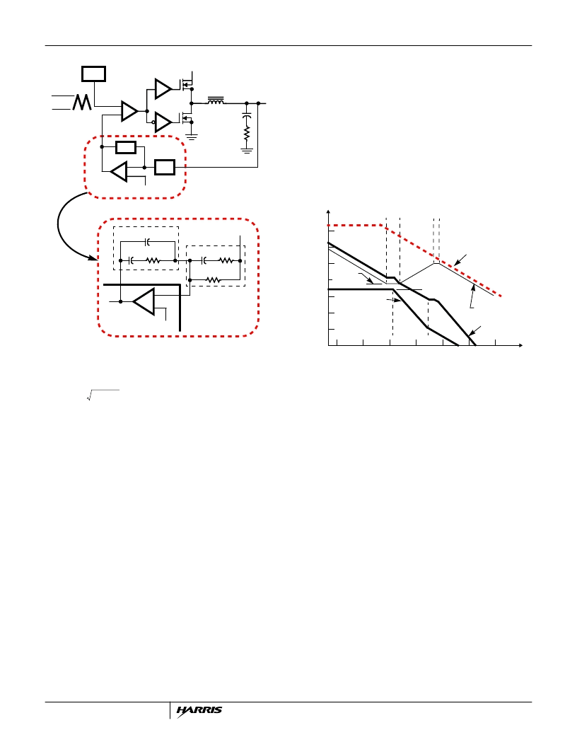
Modulator Break Frequency Equations
2
π
L
O
The compensation network consists of the error amplifier
internal to the HIP6017B and the impedance networks Z
IN
and Z
FB
. The goal of the compensation network is to provide
a closed loop transfer function with an acceptable 0dB
crossing frequency (f
0dB
) and adequate phase margin.
Phase margin is the difference between the closed loop
phase at f
0dB
and 180 degrees
.
The equations below relate
the compensation network’s poles, zeros and gain to the
components (R1, R2, R3, C1, C2, and C3) in Figure 11.
Use these guidelines for locating the poles and zeros of the
compensation network:
1. Pick Gain (R2/R1) for desired converter bandwidth
2. Place 1
ST
Zero Below Filter’s Double Pole (~75% F
LC
)
3. Place 2
ND
Zero at Filter’s Double Pole
4. Place 1
ST
Pole at the ESR Zero
5. Place 2
ND
Pole at Half the Switching Frequency
6. Check Gain against Error Amplifier’s Open-Loop Gain
7. Estimate Phase Margin - Repeat if Necessary
Compensation Break Frequency Equations
Figure 12 shows an asymptotic plot of the DC-DC
converter’s gain vs frequency. The actual modulator gain has
a peak due to the high Q factor of the output filter at F
LC
,
which is not shown in Figure 12. Using the above guidelines
should yield a compensation gain similar to the curve
plotted. The open loop error amplifier gain bounds the
compensation gain. Check the compensation gain at F
P2
with the capabilities of the error amplifier. The closed loop
gain is constructed on the log-log graph of Figure 12 by
adding the modulator gain (in dB) to the compensation gain
(in dB). This is equivalent to multiplying the modulator
transfer function to the compensation transfer function and
plotting the gain.
The compensation gain uses external impedance networks
Z
FB
and Z
IN
to provide a stable, high bandwidth loop. A
stable control loop has a 0dB gain crossing with
-20dB/decade slope and a phase margin greater than 45
degrees. Include worst case component variations when
determining phase margin.
Component Selection Guidelines
Output Capacitor Selection
The output capacitors for each output have unique
requirements. In general the output capacitors should be
selected to meet the dynamic regulation requirements.
Additionally, the PWM converters require an output capacitor
to filter the current ripple. The linear regulator is internally
compensated and requires an output capacitor that meets
the stability requirements. The load transient for the
microprocessor core requires high quality capacitors to
supply the high slew rate (di/dt) current demands.
PWM Output Capacitors
Modern microprocessors produce transient load rates above
10A/ns. High frequency capacitors initially supply the transient
and slow the current load rate seen by the bulk capacitors.
The bulk filter capacitor values are generally determined by
the ESR (effective series resistance) and ESL (effective series
inductance) parameters rather than actual capacitance.
FIGURE 11. VOLTAGE-MODE BUCK CONVERTER
COMPENSATION DESIGN
V
OUT
OSC
REFERENCE
L
O
C
O
ESR
V
IN
V
OSC
ERROR
AMP
PWM
COMP
-
DRIVER
(PARASITIC)
Z
FB
+
-
REFERENCE
R1
R3
R2
C3
C2
C1
COMP
V
OUT
FB
Z
FB
HIP6017B
Z
IN
DRIVER
DETAILED FEEDBACK COMPENSATION
PHASE
V
E/A
+
+
-
Z
IN
F
LC
C
O
×
×
---------------------------------------
=
F
ESR
O
-----------------------------------------
=
F
Z1
-----------------------------------
=
F
Z2
R3
)
C3
×
------------------------+
=
F
P1
2
π
R
2
--------+
×
×
------------------------------------------------------
=
F
P2
-----------------------------------
=
100
80
60
40
20
0
-20
-40
-60
F
P1
F
Z2
10M
1M
100K
10K
1K
100
10
OPEN LOOP
ERROR AMP GAIN
F
Z1
F
P2
20LOG
(R
2
/R
1
)
F
LC
F
ESR
COMPENSATION
GAIN
G
FREQUENCY (Hz)
20LOG
(V
IN
/
V
OSC
)
MODULATOR
GAIN
FIGURE 12. ASYMPTOTIC BODE PLOT OF CONVERTER GAIN
CLOSED LOOP
GAIN
HIP6017B
相关PDF资料 |
PDF描述 |
|---|---|
| HIP6018B | 100,000 System Gate FPGA - NOT RECOMMENDED for NEW DESIGN |
| HIP6018BCB | FPGA - 100000 SYSTEM GATE 2.5 VOLT - NOT RECOMMENDED for NEW DESIGN |
| HIP6019 | FPGA - 100000 SYSTEM GATE 2.5 VOLT - NOT RECOMMENDED for NEW DESIGN |
| HIP6019CB | Advanced Dual PWM and Dual Linear Power Control |
| HIP6019EVAL1 | Advanced Dual PWM and Dual Linear Power Control |
相关代理商/技术参数 |
参数描述 |
|---|---|
| HIP6017BCB WAF | 制造商:Harris Corporation 功能描述: |
| HIP6017BCB-T | 制造商:Rochester Electronics LLC 功能描述:- Tape and Reel |
| HIP6017CB | 制造商:Rochester Electronics LLC 功能描述:- Bulk |
| HIP6017CB WAF | 制造商:Harris Corporation 功能描述: |
| HIP6017CB-T | 制造商:Rochester Electronics LLC 功能描述:- Bulk |
发布紧急采购,3分钟左右您将得到回复。