- 您现在的位置:买卖IC网 > Datasheet目录327 > HIP6019BEVAL1 (Intersil)EVAL BOARD 1 FOR HIP6019B Datasheet资料下载
参数资料
| 型号: | HIP6019BEVAL1 |
| 厂商: | Intersil |
| 文件页数: | 10/15页 |
| 文件大小: | 0K |
| 描述: | EVAL BOARD 1 FOR HIP6019B |
| 标准包装: | 1 |
| 系列: | * |
�� �
�
�HIP6019B�
�TABLE� 1.�
�capacitors� between� the� MOSFETs� and� the� load.� Locate� the�
�PIN� NAME�
�NOMINAL�
�OUT1�
�VOLTAGE�
�PWM� controller� close� to� the� MOSFETs.�
�+5V� IN�
�VID4�
�VID3�
�VID2�
�VID1�
�VID0�
�DACOUT�
�C� IN�
�+12V�
�R�
�1�
�1�
�1�
�1�
�1�
�1�
�1�
�1�
�1�
�1�
�1�
�0�
�0�
�0�
�0�
�0�
�1�
�1�
�0�
�0�
�0�
�1�
�0�
�1�
�0�
�2.3�
�2.4�
�2.5�
�2.6�
�2.7�
�V� OUT2�
�C� OCSET2�
�R� OCSET2�
�Q3�
�L� OUT2�
�C� VCC�
�VCC� GND�
�OCSET2�
�OCSET1�
�UGATE2�
�UGATE1�
�PHASE2�
�C� OCSET1�
�OCSET1�
�Q1�
�L� OUT1�
�V� OUT1�
�1�
�0�
�1�
�1�
�1�
�2.8�
�PHASE1�
�1�
�1�
�1�
�0�
�0�
�0�
�1�
�1�
�1�
�1�
�0�
�0�
�0�
�1�
�0�
�2.9�
�3.0�
�3.1�
�C� OUT2�
�Q4�
�V� OUT3�
�HIP6019B�
�LGATE1�
�GATE3�
�SS�
�PGND�
�Q2�
�C� OUT1�
�CR1�
�1�
�1�
�1�
�1�
�0�
�0�
�0�
�0�
�0�
�0�
�0�
�0�
�1�
�1�
�0�
�0�
�1�
�0�
�1�
�0�
�3.2�
�3.3�
�3.4�
�3.5�
�C� SS�
�KEY�
�ISLAND� ON� POWER� PLANE� LAYER�
�NOTE:� 0� =� connected� to� GND� or� V� SS� ,� 1� =� open� or� connected� to� 5V�
�through� pull-up� resistors.�
�Layout� Considerations�
�MOSFETs� switch� very� fast� and� efficiently.� The� speed� with�
�which� the� current� transitions� from� one� device� to� another�
�causes� voltage� spikes� across� the� interconnecting�
�impedances� and� parasitic� circuit� elements.� The� voltage�
�spikes� can� degrade� efficiency,� radiate� noise� into� the� circuit,�
�and� lead� to� device� over-voltage� stress.� Careful� component�
�layout� and� printed� circuit� design� minimizes� the� voltage�
�spikes� in� the� converter.� Consider,� as� an� example,� the� turnoff�
�transition� of� the� upper� MOSFET.� Prior� to� turnoff,� the� upper�
�MOSFET� was� carrying� the� full� load� current.� During� the�
�turnoff,� current� stops� flowing� in� the� upper� MOSFET� and� is�
�picked� up� by� the� lower� MOSFET� or� Schottky� diode.� Any�
�inductance� in� the� switched� current� path� generates� a� large�
�voltage� spike� during� the� switching� interval.� Careful�
�component� selection,� tight� layout� of� the� critical� components,�
�and� short,� wide� circuit� traces� minimize� the� magnitude� of�
�voltage� spikes.� Contact� Intersil� for� evaluation� board�
�drawings� of� the� component� placement� and� printed� circuit�
�board.�
�There� are� two� sets� of� critical� components� in� a� DC-DC� converter�
�using� a� HIP6019B� controller.� The� power� components� are� the�
�most� critical� because� they� switch� large� amounts� of� energy.� The�
�critical� small� signal� components� connect� to� sensitive� nodes� or�
�supply� critical� bypassing� current.�
�The� power� components� should� be� placed� first.� Locate� the�
�input� capacitors� close� to� the� power� switches.� Minimize� the�
�length� of� the� connections� between� the� input� capacitors� and�
�the� power� switches.� Locate� the� output� inductor� and� output�
�10�
�ISLAND� ON� CIRCUIT� PLANE� LAYER�
�VIA� CONNECTION� TO� GROUND� PLANE�
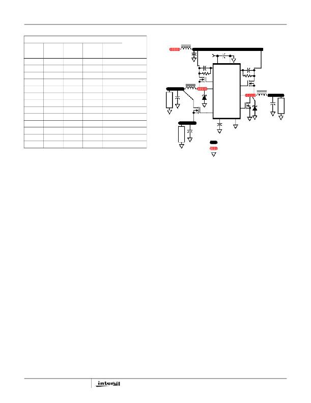
�FIGURE� 10.� PRINTED� CIRCUIT� BOARD� POWER� PLANES� AND�
�ISLANDS�
�The� critical� small� signal� components� include� the� bypass�
�capacitor� for� VCC� and� the� soft-start� capacitor,� C� SS� .� Locate�
�these� components� close� to� their� connecting� pins� on� the�
�control� IC.� Minimize� any� leakage� current� paths� from� SS�
�node� because� the� internal� current� source� is� only� 11� μ� A.�
�A� multi-layer� printed� circuit� board� is� recommended.� Figure� 10�
�shows� the� connections� of� the� critical� components� in� the�
�converter.� Note� that� capacitors� C� IN� and� C� OUT� could� each�
�represent� numerous� physical� capacitors.� Dedicate� one� solid�
�layer� for� a� ground� plane� and� make� all� critical� component�
�ground� connections� with� vias� to� this� layer.� Dedicate� another�
�solid� layer� as� a� power� plane� and� break� this� plane� into� smaller�
�islands� of� common� voltage� levels.� The� power� plane� should�
�support� the� input� power� and� output� power� nodes.� Use� copper�
�filled� polygons� on� the� top� and� bottom� circuit� layers� for� the�
�phase� nodes.� Use� the� remaining� printed� circuit� layers� for�
�small� signal� wiring.� The� wiring� traces� from� the� control� IC� to� the�
�MOSFET� gate� and� source� should� be� sized� to� carry� 1A�
�currents.� The� traces� for� OUT4� need� only� be� sized� for� 0.2A.�
�Locate� C� OUT4� close� to� the� HIP6019B� IC.�
�PWM� Controller� Feedback� Compensation�
�Both� PWM� controllers� use� voltage-mode� control� for� output�
�regulation.� This� section� highlights� the� design� consideration�
�for� a� voltage-mode� controller.� Apply� the� methods� and�
�considerations� to� both� PWM� controllers.�
�Figure� 11� highlights� the� voltage-mode� control� loop� for� a�
�synchronous-rectified� buck� converter.� The� output� voltage� is�
�regulated� to� the� reference� voltage� level.� The� reference�
�voltage� level� is� the� DAC� output� voltage� for� PWM1� and� is�
�1.265V� for� PWM2.� The� error� amplifier� output� (V� E� /A� )� is�
�FN4587.1�
�April� 13,� 2005�
�相关PDF资料 |
PDF描述 |
|---|---|
| HIP6021EVAL1 | EVALUATION BOARD HIP6021 |
| HIP6301EVAL2 | EVALUATION BOARD HIP6301 |
| HIP6302EVAL1 | EVALUATION BOARD HIP6302 |
| HIP6521EVAL1 | EVALUATION BOARD HIP6521 |
| HIP6602BCR-T | IC DRVR MOSF 2CH SYC BUCK 16-QFN |
相关代理商/技术参数 |
参数描述 |
|---|---|
| HIP6019CB | 制造商:Harris Corporation 功能描述: |
| HIP6019CB-T | 制造商:Rochester Electronics LLC 功能描述:- Bulk |
| HIP6019EVAL1 | 制造商:INTERSIL 制造商全称:Intersil Corporation 功能描述:Advanced Dual PWM and Dual Linear Power Control |
| HIP6020 | 制造商:INTERSIL 制造商全称:Intersil Corporation 功能描述:Advanced Dual PWM and Dual Linear Power Controller |
| HIP6020A | 制造商:INTERSIL 制造商全称:Intersil Corporation 功能描述:Advanced Dual PWM and Dual Linear Power Controller |
发布紧急采购,3分钟左右您将得到回复。