- 您现在的位置:买卖IC网 > PDF目录385382 > HIP6020 (Intersil Corporation) FPGA - 100000 SYSTEM GATE 2.5 VOLT - NOT RECOMMENDED for NEW DESIGN PDF资料下载
参数资料
| 型号: | HIP6020 |
| 厂商: | Intersil Corporation |
| 元件分类: | FPGA |
| 英文描述: | FPGA - 100000 SYSTEM GATE 2.5 VOLT - NOT RECOMMENDED for NEW DESIGN |
| 中文描述: | 先进的双PWM和线性双电源控制器 |
| 文件页数: | 7/15页 |
| 文件大小: | 139K |
| 代理商: | HIP6020 |
2-287
two linear controllers. The first PWM controller (PWM1) is
designed to regulate the microprocessor core voltage (V
OUT1
).
PWM1 controller drives 2 MOSFETs (Q1 and Q2) in a
synchronous-rectified buck converter and regulates the core
voltage to a level programmed by the 5-bit digital-to-analog
converter (DAC). The second PWM controller (PWM2) is
designed to regulate the advanced graphics port (AGP) bus
voltage (V
OUT2
). PWM2 controller drives a MOSFET (Q3) in a
standard buck converter and regulates the output voltage to a
digitally-programmable level of 1.5V or 3.3V. Selection of either
output voltage is achieved by applying the proper logic level at
the SELECT pin. The two linear controllers supply the 1.5V
GTL bus power (V
OUT3
) and the 1.8V memory power (V
OUT4
).
Initialization
The HIP6020 automatically initializes upon receipt of input
power. Special sequencing of the input supplies is not
necessary. The Power-On Reset (POR) function continually
monitors the input supply voltages. The POR monitors the
bias voltage (+12V
IN
) at the VCC pin, the 5V input voltage
(+5V
IN
) on the OCSET1 pin, and the 3.3V input voltage
(+3.3V
IN
) at the VAUX pin. The normal level on OCSET1 is
equal to +5V
IN
less a fixed voltage drop (see over-current
protection). The POR function initiates soft-start operation
after all supply voltages exceed their POR thresholds.
Soft-Start
The POR function initiates the soft-start sequence. Initially, the
voltage on the SS pin rapidly increases to approximately 1V
(this minimizes the soft-start interval). Then an internal 28
μ
A
current source charges an external capacitor (C
SS
) on the SS
pin to 4.5V. The PWM error amplifiers reference inputs
(+ terminal) and outputs (COMP1 pin) are clamped to a level
proportional to the SS pin voltage. As the SS pin voltage slews
from 1V to 4V, the output clamp allows generation of PHASE
pulses of increasing width that charge the output capacitor(s).
After the output voltage increases to approximately 70% of the
set value, the reference input clamp slows the output voltage
rate-of-rise and provides a smooth transition to the final set
voltage. Additionally both linear regulators’ reference inputs are
clamped to a voltage proportional to the SS pin voltage. This
method provides a rapid and controlled output voltage rise.
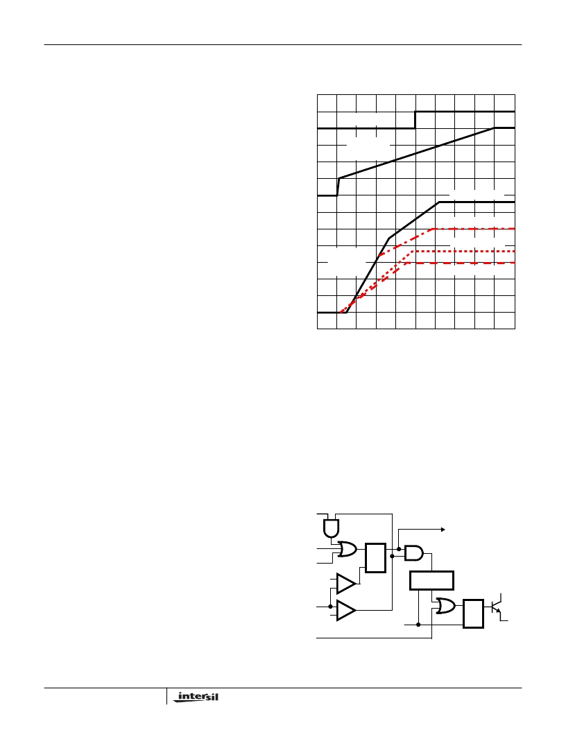
Figure 6 shows the soft-start sequence for the typical
application. At T0 the SS voltage rapidly increases to
approximately 1V. At T1, the SS pin and error amplifier
output voltage reach the valley of the oscillator’s triangle
wave. The oscillator’s triangular wave form is compared to
the clamped error amplifier output voltage. As the SS pin
voltage increases, the pulse-width on the PHASE pin
increases. The interval of increasing pulse-width continues
until each PWM output reaches sufficient voltage to transfer
control to the error amplifier input reference clamp. If we
consider the 3.3V output (V
OUT2
) in Figure 6, this time
occurs at T2. During the interval between T2 and T3, the
error amplifier reference ramps to the final value and the
converter regulates the output a voltage proportional to the
SS pin voltage. At T3 the input clamp voltage exceeds the
reference voltage and the output voltage is in regulation.
The remaining outputs are also programmed to follow the SS
pin voltage. The PGOOD signal toggles ‘high’ when all output
voltage levels have exceeded their under-voltage levels. See
the Soft-Start Interval section under Applications Guidelines
for a procedure to determine the soft-start interval.
Fault Protection
All four outputs are monitored and protected against extreme
overload. A sustained overload on any output or an over-
voltage on V
OUT1
output (VSEN1) disables all outputs and
drives the FAULT/RT pin to VCC.
FIGURE 3. SOFT-START INTERVAL
0V
0V
0V
TIME
PGOOD
SOFT-START
(1V/DIV)
OUTPUT
VOLTAGES
(0.5V/DIV)
V
OUT1
(DAC = 2.5V)
V
OUT2
( = 3.3V)
V
OUT4
( = 1.8V)
V
OUT3
( = 1.5V)
T1
T2
T3
T0
T4
FAULT
LATCH
S
R
Q
POR
COUNTER
OC1
OV
OC2
LUV
+
-
+
-
0.15V
4V
SS
VCC
FAULT
R
FIGURE 4. FAULT LOGIC - SIMPLIFIED SCHEMATIC
UP
OVER-
CURRENT
LATCH
INHIBIT
S
R
Q
HIP6020
相关PDF资料 |
PDF描述 |
|---|---|
| HIP6020CB | Advanced Dual PWM and Dual Linear Power Controller |
| HIP6301VCBZ-T | 100000 SYSTEM GATE 1.8 VOLT FPGA - NOT RECOMMENDED for NEW DESIGN |
| HIP6301VCBZA | Microprocessor CORE Voltage Regulator Multi-Phase Buck PWM Controller |
| HIP6301VCBZA-T | 150000 SYSTEM GATE 2.5 VOLT FPGA - NOT RECOMMENDED for NEW DESIGN |
| HIP6301V | Microprocessor CORE Voltage Regulator Multi-Phase Buck PWM Controller |
相关代理商/技术参数 |
参数描述 |
|---|---|
| HIP6020A | 制造商:INTERSIL 制造商全称:Intersil Corporation 功能描述:Advanced Dual PWM and Dual Linear Power Controller |
| HIP6020A_01 | 制造商:INTERSIL 制造商全称:Intersil Corporation 功能描述:Advanced Dual PWM and Dual Linear Power Controller |
| HIP6020ACB | 制造商:Intersil Corporation 功能描述: |
| HIP6020ACB WAF | 制造商:Harris Corporation 功能描述: |
| HIP6020ACB-T | 制造商:Rochester Electronics LLC 功能描述:DUAL PWM AND 2 LINEAR CONTROLLER W/O VID=11111 SHUTDOWN - Tape and Reel |
发布紧急采购,3分钟左右您将得到回复。