- 您现在的位置:买卖IC网 > PDF目录15170 > HIP6311ACBZA-T (Intersil)IC REG CTRLR BUCK PWM 20-SOIC PDF资料下载
参数资料
| 型号: | HIP6311ACBZA-T |
| 厂商: | Intersil |
| 文件页数: | 13/16页 |
| 文件大小: | 0K |
| 描述: | IC REG CTRLR BUCK PWM 20-SOIC |
| 标准包装: | 1,000 |
| PWM 型: | 控制器 |
| 输出数: | 4 |
| 频率 - 最大: | 1.5MHz |
| 电源电压: | 4.75 V ~ 5.25 V |
| 降压: | 是 |
| 升压: | 无 |
| 回扫: | 无 |
| 反相: | 无 |
| 倍增器: | 无 |
| 除法器: | 无 |
| Cuk: | 无 |
| 隔离: | 无 |
| 工作温度: | 0°C ~ 70°C |
| 封装/外壳: | 20-SOIC(0.295",7.50mm 宽) |
| 包装: | 带卷 (TR) |
�� �
�
�HIP6311A�
�As� discussed� previously,� the� voltage� drop� across� each� Q2�
�transistor� at� the� point� in� time� when� current� is� sampled� is�
�r� DSON� (Q2)� x� I� SAMPLE� .� The� voltage� at� Q2’s� drain,� the�
�PHASE� node,� is� applied� through� the� R� ISEN� resistor� to� the�
�HIP6311A� ISEN� pin.� This� pin� is� held� at� virtual� ground,� so� the�
�current� into� ISEN� is:�
�I� SENSE� =� I� SAMPLE� x� r� DS(ON)� (Q2)� /� R� ISEN� .�
�causes� voltage� spikes� across� the� interconnecting�
�impedances� and� parasitic� circuit� elements.� These� voltage�
�spikes� can� degrade� efficiency,� radiate� noise� into� the� circuit�
�and� lead� to� device� over-voltage� stress.� Careful� component�
�layout� and� printed� circuit� design� minimizes� the� voltage�
�spikes� in� the� converter.� Consider,� as� an� example,� the� turnoff�
�transition� of� the� upper� PWM� MOSFET.� Prior� to� turnoff,� the�
�upper� MOSFET� was� carrying� channel� current.� During� the�
�R� Isen�
�=� I� SAMPLE� x� r� DS(ON)� (Q2)� /� 50� μ� A�
�turnoff,� current� stops� flowing� in� the� upper� MOSFET� and� is�
�Example:� From� the� previous� conditions,�
�picked� up� by� the� lower� MOSFET.� Any� inductance� in� the�
�switched� current� path� generates� a� large� voltage� spike� during�
�where� I� LT�
�I� SAMPLE�
�r� DS(ON)� (Q2)�
�Then:� R� ISEN�
�I� CURRENT� TRIP�
�Short� circuit� I� LT�
�=� 100A,�
�=� 25.49A,�
�=� 4m� ?�
�=� 2.04K� and�
�=� 165%�
�=� 165A.�
�the� switching� interval.� Careful� component� selection,� tight�
�layout� of� the� critical� components,� and� short,� wide� circuit�
�traces� minimize� the� magnitude� of� voltage� spikes.� Contact�
�Intersil� for� evaluation� board� drawings� of� the� component�
�placement� and� printed� circuit� board.�
�There� are� two� sets� of� critical� components� in� a� DC-DC�
�converter� using� a� HIP6311A� controller� and� a� HIP6601� gate�
�driver.� The� power� components� are� the� most� critical� because�
�they� switch� large� amounts� of� energy.� Next� are� small� signal�
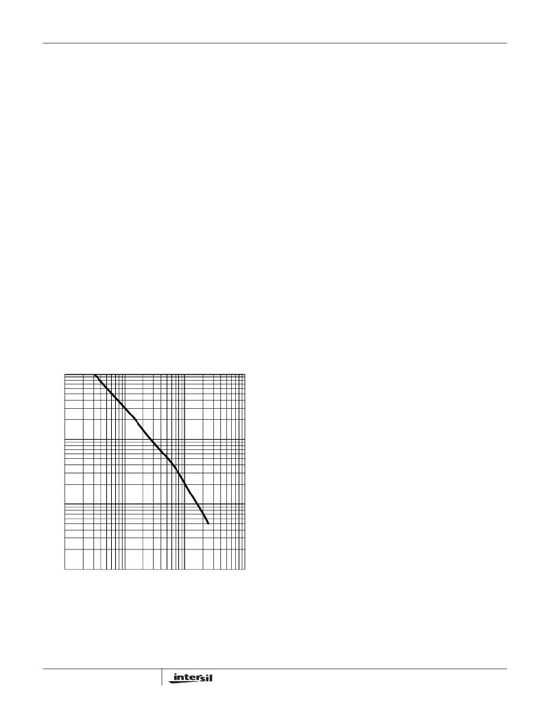
�Channel� Frequency� Oscillator�
�The� channel� oscillator� frequency� is� set� by� placing� a� resistor,�
�R� T� ,� to� ground� from� the� FS/DIS� pin.� Figure� 10� is� a� curve�
�showing� the� relationship� between� frequency,� F� SW� ,� and�
�resistor� R� T� .� To� avoid� pickup� by� the� FS/DIS� pin,� it� is� important�
�to� place� this� resistor� next� to� the� pin.� If� this� pin� is� also� used� to�
�disable� the� converter,� it� is� also� important� to� locate� the� pull-�
�down� device� next� to� this� pin.�
�1,000�
�500�
�200�
�100�
�50�
�20�
�10�
�5�
�2�
�1�
�components� that� connect� to� sensitive� nodes� or� supply� critical�
�bypassing� current� and� signal� coupling.�
�The� power� components� should� be� placed� first.� Locate� the�
�input� capacitors� close� to� the� power� switches.� Minimize� the�
�length� of� the� connections� between� the� input� capacitors,� C� IN� ,�
�and� the� power� switches.� Locate� the� output� inductors� and�
�output� capacitors� between� the� MOSFETs� and� the� load.�
�Locate� the� gate� driver� close� to� the� MOSFETs.�
�The� critical� small� components� include� the� bypass� capacitors�
�for� VCC� and� PVCC� on� the� gate� driver� ICs.� Locate� the� bypass�
�capacitor,� C� BP� ,� for� the� HIP6311A� controller� close� to� the�
�device.� It� is� especially� important� to� locate� the� resistors�
�associated� with� the� input� to� the� amplifiers� close� to� their�
�respective� pins,� since� they� represent� the� input� to� feedback�
�amplifiers.� Resistor� R� T� ,� that� sets� the� oscillator� frequency�
�should� also� be� located� next� to� the� associated� pin.� It� is�
�especially� important� to� place� the� R� SEN� resistor(s)� at� the�
�respective� terminals� of� the� HIP6311A.�
�A� multi-layer� printed� circuit� board� is� recommended.� Figure� 11�
�shows� the� connections� of� the� critical� components� for� one�
�output� channel� of� the� converter.� Note� that� capacitors� C� IN� and�
�C� OUT� could� each� represent� numerous� physical� capacitors.�
�Dedicate� one� solid� layer,� usually� the� middle� layer� of� the� PC�
�board,� for� a� ground� plane� and� make� all� critical� component�
�ground� connections� with� vias� to� this� layer.� Dedicate� another�
�solid� layer� as� a� power� plane� and� break� this� plane� into� smaller�
�10�
�20�
�50�
�100�
�200�
�500� 1,000� 2,000� 5,000� 10,000�
�islands� of� common� voltage� levels.� Keep� the� metal� runs� from�
�CHANNEL� OSCILLATOR� FREQUENCY,� F� SW� (kHz)�
�FIGURE� 10.� RESISTANCE� R� T� vs� FREQUENCY�
�Layout� Considerations�
�MOSFETs� switch� very� fast� and� efficiently.� The� speed� with�
�which� the� current� transitions� from� one� device� to� another�
�13�
�the� PHASE� terminal� to� inductor� L� O1� short.� The� power� plane�
�should� support� the� input� power� and� output� power� nodes.� Use�
�copper� filled� polygons� on� the� top� and� bottom� circuit� layers� for�
�the� phase� nodes.� Use� the� remaining� printed� circuit� layers� for�
�small� signal� wiring.� The� wiring� traces� from� the� driver� IC� to� the�
�MOSFET� gate� and� source� should� be� sized� to� carry� at� least�
�one� ampere� of� current.�
�相关PDF资料 |
PDF描述 |
|---|---|
| CAT1022WI-25-GT3 | IC SUPERVISOR CPU 2K EEPR 8SOIC |
| RBM10DRST-S273 | CONN EDGECARD 20POS DIP .156 SLD |
| CAT1021YI-45-GT3 | IC SUPERVISOR CPU 2K EEPR 8TSSOP |
| HIP6311ACBZ-T | IC REG CTRLR BUCK PWM 20-SOIC |
| EMM06DTBT-S273 | CONN EDGECARD 12POS R/A .156 SLD |
相关代理商/技术参数 |
参数描述 |
|---|---|
| HIP6311ACBZ-T | 功能描述:电流型 PWM 控制器 C4AM MULTI-PHS CONTR VID LVLS 5% AC RoHS:否 制造商:Texas Instruments 开关频率:27 KHz 上升时间: 下降时间: 工作电源电压:6 V to 15 V 工作电源电流:1.5 mA 输出端数量:1 最大工作温度:+ 105 C 安装风格:SMD/SMT 封装 / 箱体:TSSOP-14 |
| HIP6311CB | 功能描述:IC REG CTRLR BUCK PWM 20-SOIC RoHS:否 类别:集成电路 (IC) >> PMIC - 稳压器 - DC DC 切换控制器 系列:- 标准包装:4,000 系列:- PWM 型:电压模式 输出数:1 频率 - 最大:1.5MHz 占空比:66.7% 电源电压:4.75 V ~ 5.25 V 降压:是 升压:无 回扫:无 反相:无 倍增器:无 除法器:无 Cuk:无 隔离:无 工作温度:-40°C ~ 85°C 封装/外壳:40-VFQFN 裸露焊盘 包装:带卷 (TR) |
| HIP6311CB-T | 功能描述:IC REG CTRLR BUCK PWM 20-SOIC RoHS:否 类别:集成电路 (IC) >> PMIC - 稳压器 - DC DC 切换控制器 系列:- 标准包装:4,000 系列:- PWM 型:电压模式 输出数:1 频率 - 最大:1.5MHz 占空比:66.7% 电源电压:4.75 V ~ 5.25 V 降压:是 升压:无 回扫:无 反相:无 倍增器:无 除法器:无 Cuk:无 隔离:无 工作温度:-40°C ~ 85°C 封装/外壳:40-VFQFN 裸露焊盘 包装:带卷 (TR) |
| HIP6311CBZ | 功能描述:电流型 PWM 控制器 2-4 PHS SYNCH BUCK CNTRLR 0 8%F RoHS:否 制造商:Texas Instruments 开关频率:27 KHz 上升时间: 下降时间: 工作电源电压:6 V to 15 V 工作电源电流:1.5 mA 输出端数量:1 最大工作温度:+ 105 C 安装风格:SMD/SMT 封装 / 箱体:TSSOP-14 |
| HIP6311CBZA | 功能描述:电流型 PWM 控制器 W/ANL 2-4 PHS SYNCH BUCK CNTRLR 0 8%F RoHS:否 制造商:Texas Instruments 开关频率:27 KHz 上升时间: 下降时间: 工作电源电压:6 V to 15 V 工作电源电流:1.5 mA 输出端数量:1 最大工作温度:+ 105 C 安装风格:SMD/SMT 封装 / 箱体:TSSOP-14 |
发布紧急采购,3分钟左右您将得到回复。