- 您现在的位置:买卖IC网 > PDF目录15170 > HIP6311ACBZA-T (Intersil)IC REG CTRLR BUCK PWM 20-SOIC PDF资料下载
参数资料
| 型号: | HIP6311ACBZA-T |
| 厂商: | Intersil |
| 文件页数: | 15/16页 |
| 文件大小: | 0K |
| 描述: | IC REG CTRLR BUCK PWM 20-SOIC |
| 标准包装: | 1,000 |
| PWM 型: | 控制器 |
| 输出数: | 4 |
| 频率 - 最大: | 1.5MHz |
| 电源电压: | 4.75 V ~ 5.25 V |
| 降压: | 是 |
| 升压: | 无 |
| 回扫: | 无 |
| 反相: | 无 |
| 倍增器: | 无 |
| 除法器: | 无 |
| Cuk: | 无 |
| 隔离: | 无 |
| 工作温度: | 0°C ~ 70°C |
| 封装/外壳: | 20-SOIC(0.295",7.50mm 宽) |
| 包装: | 带卷 (TR) |
�� �
�
�HIP6311A�
�Considerations� section.� With� all� else� fixed,� decreasing� the�
�inductance� could� increase� the� power� dissipated� in� the�
�MOSFETs� by� 30%.�
�1.0�
�the� high� frequency� decoupling� and� bulk� capacitors� to� supply�
�the� RMS� current.� Small� ceramic� capacitors� should� be� placed�
�very� close� to� the� drain� of� the� upper� MOSFET� to� suppress� the�
�voltage� induced� in� the� parasitic� circuit� impedances.�
�For� bulk� capacitance,� several� electrolytic� capacitors�
�0.8�
�SINGLE�
�CHANNEL�
�(Panasonic� HFQ� series� or� Nichicon� PL� series� or� Sanyo�
�MV-GX� or� equivalent)� may� be� needed.� For� surface� mount�
�designs,� solid� tantalum� capacitors� can� be� used,� but� caution�
�0.6�
�0.4�
�0.2�
�3 CHANNEL�
�4 CHANNEL�
�2 CHANNEL�
�must� be� exercised� with� regard� to� the� capacitor� surge� current�
�rating.� These� capacitors� must� be� capable� of� handling� the�
�surge-current� at� power-up.� The� TPS� series� available� from�
�AVX,� and� the� 593D� series� from� Sprague� are� both� surge�
�current� tested.�
�MOSFET� Selection� and� Considerations�
�0�
�0�
�0.1�
�0.2� 0.3�
�DUTY� CYCLE� (V� O� /V� IN� )�
�0.4�
�0.5�
�In� high-current� PWM� applications,� the� MOSFET� power�
�dissipation,� package� selection� and� heatsink� are� the�
�dominant� design� factors.� The� power� dissipation� includes� two�
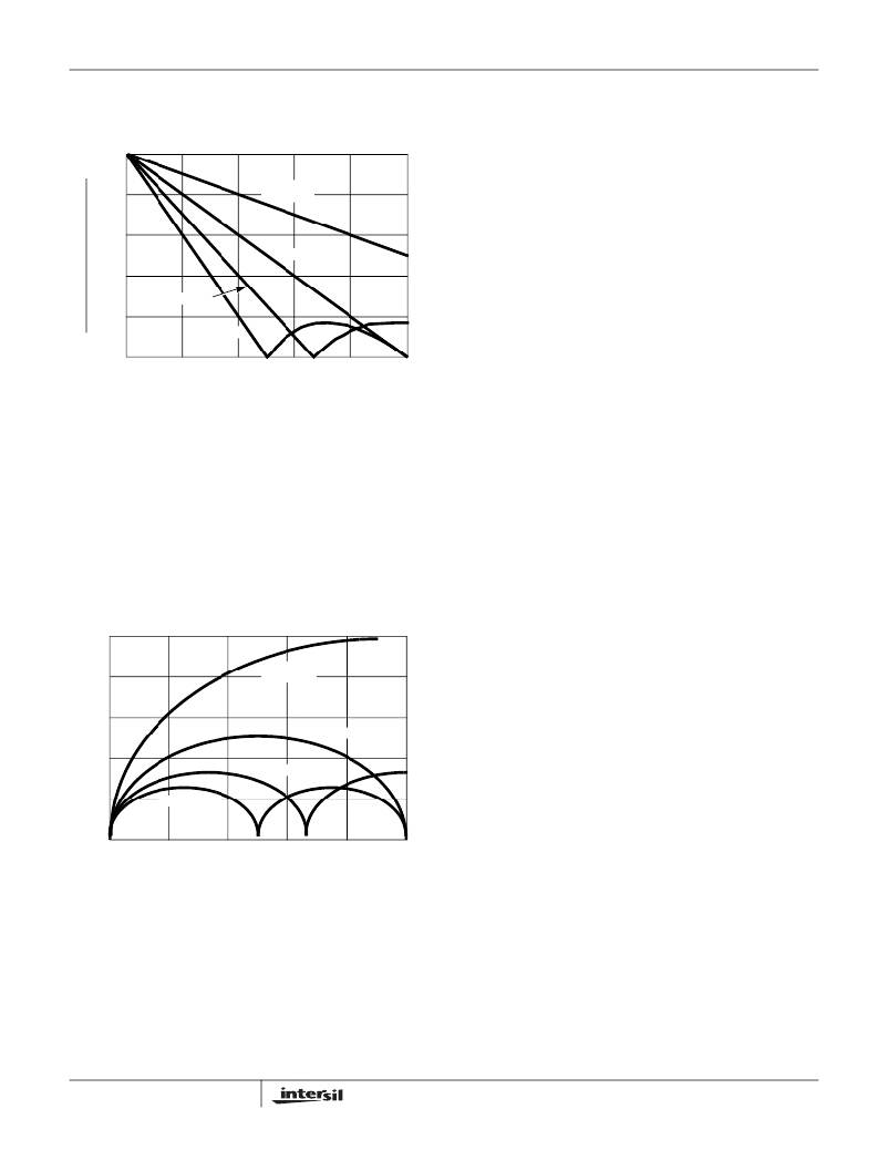
�FIGURE� 12.� RIPPLE� CURRENT� vs� DUTY� CYCLE�
�Input� Capacitor� Selection�
�The� important� parameters� for� the� bulk� input� capacitors� are� the�
�voltage� rating� and� the� RMS� current� rating.� For� reliable�
�operation,� select� bulk� input� capacitors� with� voltage� and� current�
�ratings� above� the� maximum� input� voltage� and� largest� RMS�
�current� required� by� the� circuit.� The� capacitor� voltage� rating�
�should� be� at� least� 1.25� times� greater� than� the� maximum� input�
�voltage� and� a� voltage� rating� of� 1.5� times� is� a� conservative�
�guideline.� The� RMS� current� required� for� a� multi-phase�
�converter� can� be� approximated� with� the� aid� of� Figure� 13.�
�0.5�
�SINGLE�
�loss� components;� conduction� loss� and� switching� loss.� These�
�losses� are� distributed� between� the� upper� and� lower�
�MOSFETs� according� to� duty� factor� (see� the� following�
�equations).� The� conduction� losses� are� the� main� component�
�of� power� dissipation� for� the� lower� MOSFETs,� Q2� and� Q4� of�
�Figure� 1.� Only� the� upper� MOSFETs,� Q1� and� Q3� have�
�significant� switching� losses,� since� the� lower� device� turns� on�
�and� off� into� near� zero� voltage.�
�The� equations� assume� linear� voltage-current� transitions� and�
�do� not� model� power� loss� due� to� the� reverse-recovery� of� the�
�lower� MOSFETs� body� diode.� The� gate-charge� losses� are�
�dissipated� by� the� Driver� IC� and� don't� heat� the� MOSFETs.�
�However,� large� gate-charge� increases� the� switching� time,�
�t� SW� which� increases� the� upper� MOSFET� switching� losses.�
�Ensure� that� both� MOSFETs� are� within� their� maximum�
�0.4�
�CHANNEL�
�junction� temperature� at� high� ambient� temperature� by�
�calculating� the� temperature� rise� according� to� package�
�0.3�
�0.2�
�2 CHANNEL�
�thermal-resistance� specifications.� A� separate� heatsink� may�
�be� necessary� depending� upon� MOSFET� power,� package�
�type,� ambient� temperature� and� air� flow.�
�I� O� � r� DS� (� ON� )� � V� OUT�
�I� O� � V� IN� � t� SW� � F� SW�
�P� UPPER� =� ------------------------------------------------------------� +� ----------------------------------------------------------�
�V� IN�
�0.1�
�4 CHANNEL�
�3� CHANNEL�
�2�
�2�
�I� O� ×� r� DS� (� ON� )� ×� (� V� IN� –� V� OUT� )�
�V� IN�
�0�
�0�
�0.1�
�0.2�
�0.3�
�0.4�
�0.5�
�2�
�P� LOWER� =� ---------------------------------------------------------------------------------�
�DUTY� CYCLE� (V� O� /V� IN� )�
�FIGURE� 13.� CURRENT� MULTIPLIER� vs� DUTY� CYCLE�
�First� determine� the� operating� duty� ratio� as� the� ratio� of� the�
�output� voltage� divided� by� the� input� voltage.� Find� the� Current�
�Multiplier� from� the� curve� with� the� appropriate� power�
�channels.� Multiply� the� current� multiplier� by� the� full� load�
�output� current.� The� resulting� value� is� the� RMS� current� rating�
�required� by� the� input� capacitor.�
�Use� a� mix� of� input� bypass� capacitors� to� control� the� voltage�
�overshoot� across� the� MOSFETs.� Use� ceramic� capacitance� for�
�15�
�A� diode,� anode� to� ground,� may� be� placed� across� Q2� and� Q4.�
�These� diodes� function� as� a� clamp� that� catches� the� negative�
�inductor� swing� during� the� dead� time� between� the� turn� off� of�
�the� lower� MOSFETs� and� the� turn� on� of� the� upper� MOSFETs.�
�The� diodes� must� be� a� Schottky� type� to� prevent� the� lossy�
�parasitic� MOSFET� body� diode� from� conducting.� It� is� usually�
�acceptable� to� omit� the� diodes� and� let� the� body� diodes� of� the�
�lower� MOSFETs� clamp� the� negative� inductor� swing,� but�
�efficiency� could� drop� one� or� two� percent� as� a� result.� The�
�diode's� rated� reverse� breakdown� voltage� must� be� greater�
�than� the� maximum� input� voltage.�
�相关PDF资料 |
PDF描述 |
|---|---|
| CAT1022WI-25-GT3 | IC SUPERVISOR CPU 2K EEPR 8SOIC |
| RBM10DRST-S273 | CONN EDGECARD 20POS DIP .156 SLD |
| CAT1021YI-45-GT3 | IC SUPERVISOR CPU 2K EEPR 8TSSOP |
| HIP6311ACBZ-T | IC REG CTRLR BUCK PWM 20-SOIC |
| EMM06DTBT-S273 | CONN EDGECARD 12POS R/A .156 SLD |
相关代理商/技术参数 |
参数描述 |
|---|---|
| HIP6311ACBZ-T | 功能描述:电流型 PWM 控制器 C4AM MULTI-PHS CONTR VID LVLS 5% AC RoHS:否 制造商:Texas Instruments 开关频率:27 KHz 上升时间: 下降时间: 工作电源电压:6 V to 15 V 工作电源电流:1.5 mA 输出端数量:1 最大工作温度:+ 105 C 安装风格:SMD/SMT 封装 / 箱体:TSSOP-14 |
| HIP6311CB | 功能描述:IC REG CTRLR BUCK PWM 20-SOIC RoHS:否 类别:集成电路 (IC) >> PMIC - 稳压器 - DC DC 切换控制器 系列:- 标准包装:4,000 系列:- PWM 型:电压模式 输出数:1 频率 - 最大:1.5MHz 占空比:66.7% 电源电压:4.75 V ~ 5.25 V 降压:是 升压:无 回扫:无 反相:无 倍增器:无 除法器:无 Cuk:无 隔离:无 工作温度:-40°C ~ 85°C 封装/外壳:40-VFQFN 裸露焊盘 包装:带卷 (TR) |
| HIP6311CB-T | 功能描述:IC REG CTRLR BUCK PWM 20-SOIC RoHS:否 类别:集成电路 (IC) >> PMIC - 稳压器 - DC DC 切换控制器 系列:- 标准包装:4,000 系列:- PWM 型:电压模式 输出数:1 频率 - 最大:1.5MHz 占空比:66.7% 电源电压:4.75 V ~ 5.25 V 降压:是 升压:无 回扫:无 反相:无 倍增器:无 除法器:无 Cuk:无 隔离:无 工作温度:-40°C ~ 85°C 封装/外壳:40-VFQFN 裸露焊盘 包装:带卷 (TR) |
| HIP6311CBZ | 功能描述:电流型 PWM 控制器 2-4 PHS SYNCH BUCK CNTRLR 0 8%F RoHS:否 制造商:Texas Instruments 开关频率:27 KHz 上升时间: 下降时间: 工作电源电压:6 V to 15 V 工作电源电流:1.5 mA 输出端数量:1 最大工作温度:+ 105 C 安装风格:SMD/SMT 封装 / 箱体:TSSOP-14 |
| HIP6311CBZA | 功能描述:电流型 PWM 控制器 W/ANL 2-4 PHS SYNCH BUCK CNTRLR 0 8%F RoHS:否 制造商:Texas Instruments 开关频率:27 KHz 上升时间: 下降时间: 工作电源电压:6 V to 15 V 工作电源电流:1.5 mA 输出端数量:1 最大工作温度:+ 105 C 安装风格:SMD/SMT 封装 / 箱体:TSSOP-14 |
发布紧急采购,3分钟左右您将得到回复。