- 您现在的位置:买卖IC网 > PDF目录370643 > HMP8112EVAL2 (Harris Corporation) NTSC/PAL Video Decoder PDF资料下载
参数资料
| 型号: | HMP8112EVAL2 |
| 厂商: | Harris Corporation |
| 英文描述: | NTSC/PAL Video Decoder |
| 中文描述: | NTSC / PAL视频解码器 |
| 文件页数: | 11/40页 |
| 文件大小: | 563K |
| 代理商: | HMP8112EVAL2 |
第1页第2页第3页第4页第5页第6页第7页第8页第9页第10页当前第11页第12页第13页第14页第15页第16页第17页第18页第19页第20页第21页第22页第23页第24页第25页第26页第27页第28页第29页第30页第31页第32页第33页第34页第35页第36页第37页第38页第39页第40页
11
The 2-bit values allow 4 choices of scaling factors. The
sharpness control helps to compensate for losses in the
scaling interpolators that can reduce the amplitude of high
frequency components.
The Color Killer
(AGC Hysteresis and Loop Limits)
The color killer will disable the color difference path and set
the U and V components to zero. The automatic color killer
circuitry uses the AGC threshold to determine the maximum
and minimum gain factor limits. The loop filter determines
how much the AGC gain factor can be changed within one
line. The maximum gain factor (Max = 8) and the minimum
gain factor (Min = 0.5) will limit the range of the AGC. When
the gain factor exceeds the maximum gain factor of 8, the
gain factor is limited to 8. Once the signal has an amplitude
of 1/16th, the nominal video the color killer is enabled and
the chroma phase locked loop holds it’s last phase refer-
ence. While the color killer is enabled, the U and V compo-
nents are forced to zero. Once the input video signal reaches
1/7th the optimum amplitude the color killer is disabled and
the color is returned.
The dynamic range of the AGC allows it to compensate for
video that is 1/8 to 2 times the specified nominal of 1V
P-P
.
Saturation
The color saturation component is controlled via the Color
Saturation Registers. The color saturation is applied to the
UV components after the AGC function. The saturation value
is multiplied by the UV data to increase the color intensity.
The data range is from 0 to 1.96875 where 1.96875 is the
brightest intensity. This is an 8-bit number in the form:
X.XXX XXXX
The default value after a RESET is 1.2074 (9D
H
).
I
2
C Control Interface
The HMP8112 utilizes an I
2
C control bus interface to pro-
gram the internal configuration registers. This standard
mode (up to 100 KBPS) interface consists of the bidirec-
tional Serial Data Line (SDA) and the Serial Clock Line
(SCL). The implementation on the HMP8112 is a simple
slave interface that will not respond to general calls and can-
not initiate a transfer. When the device is not active, the SDA
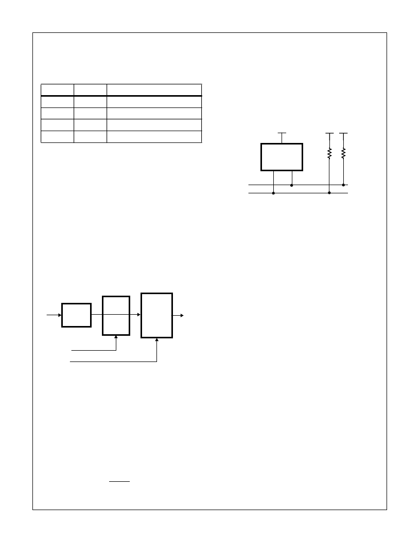
and SCL control pins should be pulled high through external
4k
pullup resistors.
The I
2
C clock/data timing is shown below in Figure 13. The
HMP8112 contains 29 internal registers used to program and
configure the Decoder. The I
2
C control port contains a pointer
register that auto-increments through the entire register space
and can be written. The autoincrement pointer will wrap after
the last register has been accessed (Product ID Register) and
should be set to the desired starting address each time an
access is started. For a write transfer, the I
2
C device base
address is the first part of a serial transfer. Then the internal
register pointer is loaded. Then a series of registers can be
written. If multiple registers are written, the pointer register will
autoincrement up through the register address space. A stop
cycle is used to end the transfer after the desired number of
registers are programmed.
For a read transfer, the I
2
C device address is the first part of
the serial transfer. Then the internal register pointer is
loaded. At this point another start cycle is initiated to access
the individual registers. Figure 14 shows the programming
flow for read transfer of the internal registers. Multiple regis-
ters can be read and the pointer register will autoincrement
up through the pointer register address space. On the last
data read, an acknowledge should not be issued. A stop
cycle is used to end the transfer after the desired number of
registers are read.
Product ID Register
The HMP8112 contains a product ID register that can be
used to identify the presence of a board during a Plug ’n Play
detection software algorithm. The Product ID code is 12
H
and the register is the last register in the HMP8112 (1B
H
).
Output Data Port Modes
The HMP8112 can output data in 2 formats, an 8-bit Burst
mode and a 16-bit Synchronous Pixel Transfer mode. In 16-bit
Synchronous Pixel Transfer Mode pixel data is output at the
TABLE 4. SHARPNESS GAIN FACTOR SELECTS
XF1
XF0
GAIN FACTOR
0
0
SCALED BY 1.0
0
1
SCALED BY 2.0
1
0
SCALED BY 4.0
1
1
SCALED BY 0
÷
4096
FACTOR
GAIN
MIN
I
2
C
COLOR
KILLER
LINE
COUNT
UV
DATA
AGC
ENABLE
FIGURE 11. LOOP FILTER BLOCK DIAGRAM (HYSTERESIS)
FACTOR
GAIN
MAX
AGC
GAIN
FACTOR
+5V
HMP8112
VIDEO
DECODER
+5V
SDA
SCL
+5V
40
41
4k
4k
FIGURE 12. PULLUP RESISTOR CONFIGURATION
HMP8112
相关PDF资料 |
PDF描述 |
|---|---|
| HMP8156EVAL2 | NTSC/PAL Video Decoder |
| HMP8156EVAL1 | NTSC/PAL Encoders |
| HMP8156EVAL2 | NTSC/PAL Encoders |
| HMP8156 | NTSC/PAL Encoder |
| HMP8156ACN | NTSC/PAL Encoders |
相关代理商/技术参数 |
参数描述 |
|---|---|
| HMP8115 | 制造商:INTERSIL 制造商全称:Intersil Corporation 功能描述:NTSC/PAL Video Decoder |
| HMP8115CN | 制造商:INTERSIL 制造商全称:Intersil Corporation 功能描述:NTSC/PAL Video Decoder |
| HMP8116 | 制造商:INTERSIL 制造商全称:Intersil Corporation 功能描述:NTSC/PAL Video Decoder |
| HMP8116CN | 制造商:INTERSIL 制造商全称:Intersil Corporation 功能描述:NTSC/PAL Video Decoder |
| HMP8117 | 制造商:INTERSIL 制造商全称:Intersil Corporation 功能描述:NTSC/PAL Video Decoder |
发布紧急采购,3分钟左右您将得到回复。