- 您现在的位置:买卖IC网 > Datasheet目录327 > HW-V5-ML501-UNI-G (Xilinx Inc)EVALUATION PLATFORM VIRTEX-5 Datasheet资料下载
参数资料
| 型号: | HW-V5-ML501-UNI-G |
| 厂商: | Xilinx Inc |
| 文件页数: | 34/42页 |
| 文件大小: | 0K |
| 描述: | EVALUATION PLATFORM VIRTEX-5 |
| 产品变化通告: | Adapter Replacement 23/May/2008 |
| 设计资源: | ML501 Ref Design User Guide ML501 Schematics |
| 标准包装: | 1 |
| 系列: | Virtex®-5 LX |
| 类型: | FPGA |
| 适用于相关产品: | XC5VLX50FFG676 |
| 所含物品: | ML501 平台、DVI 适配器和 CompactFlash 卡 |
| 相关产品: | XC5VLX50T-3FFG665C-ND - IC FPGA VIRTEX-5 50K 665FCBGA XC5VLX50T-3FFG1136C-ND - IC FPGA VIRTEX-5 50K 1136FBGA XC5VLX50T-3FF665C-ND - IC FPGA VIRTEX-5 50K 665FCBGA XC5VLX50T-3FF1136C-ND - IC FPGA VIRTEX-5 50K 1136FBGA XC5VLX50T-2FFG665I-ND - IC FPGA VIRTEX-5 50K 665FCBGA XC5VLX50T-2FFG665C-ND - IC FPGA VIRTEX-5 50K 665FCBGA XC5VLX50T-2FFG1136I-ND - IC FPGA VIRTEX-5 50K 1136FBGA XC5VLX50T-2FFG1136C-ND - IC FPGA VIRTEX-5 50K 1136FBGA XC5VLX50T-2FF665I-ND - IC FPGA VIRTEX-5 50K 665FCBGA XC5VLX50T-2FF665C-ND - IC FPGA VIRTEX-5 50K 665FCBGA 更多... |
| 其它名称: | 122-1508 |
第1页第2页第3页第4页第5页第6页第7页第8页第9页第10页第11页第12页第13页第14页第15页第16页第17页第18页第19页第20页第21页第22页第23页第24页第25页第26页第27页第28页第29页第30页第31页第32页第33页当前第34页第35页第36页第37页第38页第39页第40页第41页第42页
�� �
�
�Chapter� 1:� ML501� Evaluation� Platform�
�R�
�3� 7.� System� Monitor�
�The� ML501� supports� both� the� dedicated� and� the� auxiliary� analog� inputs� to� the� Virtex-5�
�FPGA� System� Monitor� block.� The� VP� and� VN� pins� shown� in� Table� 1-16,� page� 34� are� the�
�dedicated� pins,� whereas� the� VAUXP[� x� ],� VAUXN[� x� ]� represent� the� 16� user-selectable�
�auxiliary� analog� input� channels.� The� ML501� PCB� layout� for� the� VP� and� VN� pins� is�
�designed� using� differential� pairs� and� anti-alias� filtering� in� close� proximity� to� the� FPGA� as�
�recommended� in� the� Virtex-5� FPGA� System� Monitor� User� Guide� [Ref� 8]� .� Please� note� that� the�
�circuitry� connected� to� the� 16� AUX� channels� on� the� ML501� are� connected� in� a� non-optimal�
�fashion� as� they� are� implemented� without� anti-alias� filtering� at� the� FPGA.� This� tradeoff� was�
�made� as� the� AUX� channels� are� also� used� as� general-purpose� I/O� on� the� XGI� connectors�
�(see� “10.� XGI� Expansion� Headers,”� page� 20� for� additional� details).� The� AUX� channels� are�
�still� available� for� use� with� the� System� Monitor� functions,� but� they� will� not� attain� the�
�performance� level� of� the� dedicated� analog� input� as� noted� in� the� Virtex-5� FPGA� System�
�Monitor� User� Guide� .� Access� to� the� dedicated� analog� input� pairs� (VP/VN)� is� provided�
�through� pins� 9� and� 10� of� the� System� Monitor� Header� (J15).� See� Table� 1-16� .�
�The� Virtex-5� FPGA� System� Monitor� function� is� built� around� a� 10-bit,� 200-kSPS�
�(kilosamples� per� second)� Analog-to-Digital� Converter� (ADC).� When� combined� with� a�
�number� of� on-chip� sensors,� the� ADC� is� used� to� measure� FPGA� physical� operating�
�parameters� like� on-chip� power� supply� voltages� and� die� temperatures.� Access� to� external�
�voltages� is� provided� through� a� dedicated� analog-input� pair� (VP/VN)� and� 16� user�
�selectable� analog� inputs,� known� as� auxiliary� analog� inputs� (VAUXP[15:0],� VAUXN[15:0]).�
�The� System� Monitor� is� fully� functional� on� power� up,� and� measurement� data� can� be�
�accessed� via� the� JTAG� port� pre-configuration.� The� Xilinx� ChipScope?� Pro tool� provides�
�access� to� the� System� Monitor� over� the� JTAG� port.� The� System� Monitor� control� logic�
�implements� some� common� monitoring� features.� For� example,� an� automatic� channel�
�sequencer� allows� a� user-defined� selection� of� parameters� to� be� automatically� monitored,�
�and� user-programmable� averaging� is� enabled� to� ensure� robust� noise-free� measurements.�
�The� System� Monitor� also� provides� user-programmable� alarm� thresholds� for� the� on-chip�
�sensors.� Thus,� if� an� on-chip� monitored� parameter� moves� outside� the� user-specified�
�operating� range,� an� alarm� logic� output� becomes� active.� In� addition� to� monitoring� the� on-�
�chip� temperature� for� user-defined� applications,� the� System� Monitor� issues� a� special� alarm�
�called� Over-Temperature� (OT)� if� the� FPGA� temperature� becomes� critical� (>� 125°C).� The�
�over-temperature� signal� is� deactivated� when� the� device� temperature� falls� below� a� user-�
�specified� lower� limit.� If� the� FPGA� power-down� feature� is� enabled,� the� FPGA� enters� power�
�down� when� the� OT� signal� becomes� active.� The� FPGA� powers� up� again� when� the� alarm� is�
�deactivated.�
�For� additional� information� about� the� System� Monitor,� see�
�http://www.xilinx.com/systemmonitor� and� consult� the� Virtex-5� FPGA� System� Monitor�
�User� Guide� [Ref� 8]� .� Table� 1-16� shows� the� System� Monitor� connections.�
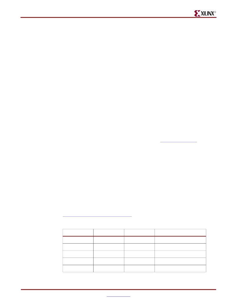
�Table� 1-16:�
�System� Monitor� Connections�
�External� Input�
�VN�
�VP�
�VAUXN[0]�
�VAUXP[0]�
�VAUXN[1]�
�FPGA� Pin�
�P13�
�N14�
�N24�
�M24�
�M26�
�Header� Pin�
�J15-10�
�J15-9�
�J6-30�
�J6-32�
�J6-26�
�Schematic� Net� Name�
�FPGA_V_N�
�FPGA_V_P�
�HDR1_30_SM_0_N�
�HDR1_32_SM_0_P�
�HDR1_26_SM_1_N�
�34�
��ML501� Evaluation� Platform�
�UG226� (v1.4)� August� 24,� 2009�
�相关PDF资料 |
PDF描述 |
|---|---|
| HW-V5-ML507-UNI-G | EVAL PLATFORM V5 FXT |
| HW-V5-ML550-UNI-G | EVALUATION PLATFORM VIRTEX-5 |
| HW-V5-ML555-G | BOARD EVAL FOR VIRTEX-5 ML555 |
| HW-V5-ML561-UNI-G | EVALUATION PLATFORM VIRTEX-5 |
| I-JET | JTAG ARM DEBUGGING PROBE |
相关代理商/技术参数 |
参数描述 |
|---|---|
| HW-V5-ML501-UNI-G-J | 功能描述:EVALUATION PLATFORM VIRTEX-5 RoHS:是 类别:编程器,开发系统 >> 通用嵌入式开发板和套件(MCU、DSP、FPGA、CPLD等) 系列:Virtex®-5 LX 标准包装:1 系列:PICDEM™ 类型:MCU 适用于相关产品:PIC10F206,PIC16F690,PIC16F819 所含物品:板,线缆,元件,CD,PICkit 编程器 产品目录页面:659 (CN2011-ZH PDF) |
| HW-V5-ML505-UNI-G | 制造商:Xilinx 功能描述:HARDWARE, VIRTEX-5 ML505 EVALUATION PLATFORM, UNIVERSAL - Bulk 制造商:Xilinx 功能描述:XLXHW-V5-ML505-UNI-G EVALUATION KIT 制造商:Xilinx 功能描述:KIT EVAL PLATFORM VIRTEX-5 LXT ML505 |
| HW-V5-ML505-UNI-G-J | 功能描述:VIRTEX-5 LXT ML505 EVAL PLATFORM RoHS:是 类别:编程器,开发系统 >> 通用嵌入式开发板和套件(MCU、DSP、FPGA、CPLD等) 系列:Virtex®-5 LXT 标准包装:1 系列:PICDEM™ 类型:MCU 适用于相关产品:PIC10F206,PIC16F690,PIC16F819 所含物品:板,线缆,元件,CD,PICkit 编程器 产品目录页面:659 (CN2011-ZH PDF) |
| HW-V5-ML506-UNI-G | 功能描述:EVALUATION PLATFORM VIRTEX-5 RoHS:是 类别:编程器,开发系统 >> 通用嵌入式开发板和套件(MCU、DSP、FPGA、CPLD等) 系列:Virtex®-5 SXT 标准包装:1 系列:PICDEM™ 类型:MCU 适用于相关产品:PIC10F206,PIC16F690,PIC16F819 所含物品:板,线缆,元件,CD,PICkit 编程器 产品目录页面:659 (CN2011-ZH PDF) |
| HW-V5-ML506-UNI-G-J | 功能描述:EVALUATION PLATFORM VIRTEX-5 RoHS:是 类别:编程器,开发系统 >> 通用嵌入式开发板和套件(MCU、DSP、FPGA、CPLD等) 系列:Virtex®-5 SXT 标准包装:1 系列:PICDEM™ 类型:MCU 适用于相关产品:PIC10F206,PIC16F690,PIC16F819 所含物品:板,线缆,元件,CD,PICkit 编程器 产品目录页面:659 (CN2011-ZH PDF) |
发布紧急采购,3分钟左右您将得到回复。