- 您现在的位置:买卖IC网 > PDF目录17028 > HW-V5-PCIE2-UNI-G (Xilinx Inc)KIT DEV PCIEXPRESS GTX VIRTEX5 PDF资料下载
参数资料
| 型号: | HW-V5-PCIE2-UNI-G |
| 厂商: | Xilinx Inc |
| 文件页数: | 12/91页 |
| 文件大小: | 0K |
| 描述: | KIT DEV PCIEXPRESS GTX VIRTEX5 |
| 产品培训模块: | PCI Express and Virtex® -5 FPGAs |
| 标准包装: | 1 |
| 系列: | Virtex® -5 |
| 类型: | FPGA |
| 适用于相关产品: | Virtex?-5 FPGA |
| 所含物品: | 板,CD |
第1页第2页第3页第4页第5页第6页第7页第8页第9页第10页第11页当前第12页第13页第14页第15页第16页第17页第18页第19页第20页第21页第22页第23页第24页第25页第26页第27页第28页第29页第30页第31页第32页第33页第34页第35页第36页第37页第38页第39页第40页第41页第42页第43页第44页第45页第46页第47页第48页第49页第50页第51页第52页第53页第54页第55页第56页第57页第58页第59页第60页第61页第62页第63页第64页第65页第66页第67页第68页第69页第70页第71页第72页第73页第74页第75页第76页第77页第78页第79页第80页第81页第82页第83页第84页第85页第86页第87页第88页第89页第90页第91页
Virtex-5 FPGA Data Sheet: DC and Switching Characteristics
DS202 (v5.3) May 5, 2010
Product Specification
2
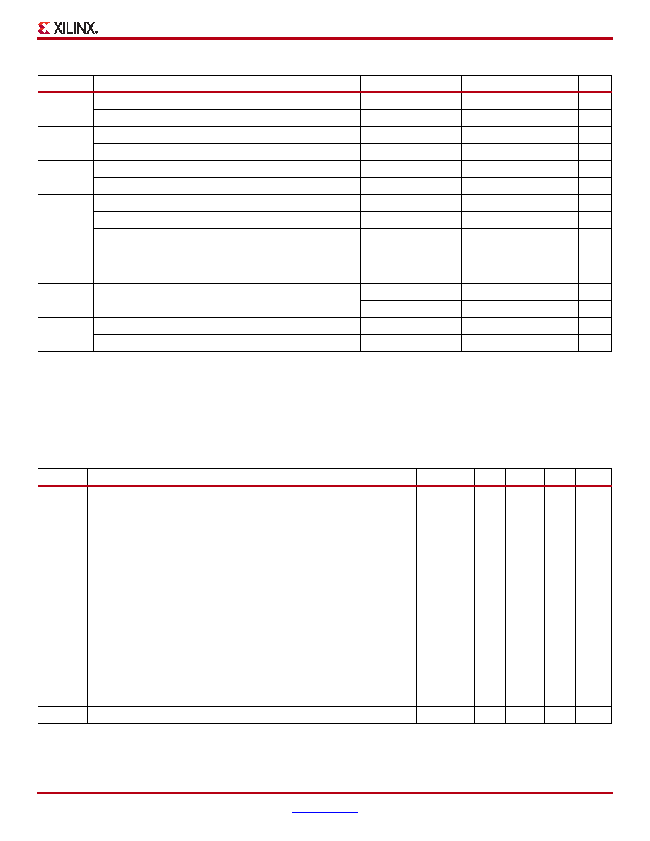
Table 2: Recommended Operating Conditions
Symbol
Description
Temperature Range
Min
Max
Units
VCCINT
Internal supply voltage relative to GND, TJ =0°C to +85°C
Commercial
0.95
1.05
V
Internal supply voltage relative to GND, TJ = –40°C to +100°C
Industrial
0.95
1.05
V
VCCAUX(1)
Auxiliary supply voltage relative to GND, TJ =0°C to +85°C
Commercial
2.375
2.625
V
Auxiliary supply voltage relative to GND, TJ =–40°C to +100°C
Industrial
2.375
2.625
V
VCCO(2,4,5)
Supply voltage relative to GND, TJ =0°C to +85°C
Commercial
1.14
3.45
V
Supply voltage relative to GND, TJ =–40°C to +100°C
Industrial
1.14
3.45
V
VIN
3.3V supply voltage relative to GND, TJ =0°C to +85°C
Commercial
GND – 0.20
3.45
V
3.3V supply voltage relative to GND, TJ = –40°C to +100°C
Industrial
GND – 0.20
3.45
V
2.5V and below supply voltage relative to GND,
TJ =0°C to +85°C
Commercial
GND – 0.20
VCCO + 0.2
V
2.5V and below supply voltage relative to GND,
TJ = –40°C to +100°C
Industrial
GND – 0.20
VCCO + 0.2
V
IIN(6)
Maximum current through any pin in a powered or unpowered
bank when forward biasing the clamp diode
Commercial
10
mA
Industrial
10
mA
VBATT(3)
Battery voltage relative to GND, TJ =0°C to +85°C
Commercial
1.0
3.6
V
Battery voltage relative to GND, TJ =–40°C to +100°C
Industrial
1.0
3.6
V
Notes:
1.
Recommended maximum voltage drop for VCCAUX is 10 mV/ms.
2.
Configuration data is retained even if VCCO drops to 0V.
3.
VBATT is required only when using bitstream encryption. If battery is not used, connect VBATT to either ground or VCCAUX.
4.
Includes VCCO of 1.2V, 1.5V, 1.8V, 2.5V, and 3.3V.
5.
The configuration supply voltage VCC_CONFIG is also known as VCCO_0.
6.
A total of 100 mA per bank should not be exceeded.
Table 3: DC Characteristics Over Recommended Operating Conditions
Symbol
Description
Data Rate
Min
Typ
Max
Units
VDRINT
Data retention VCCINT voltage (below which configuration data might be lost)
0.75
V
VDRI
Data retention VCCAUX voltage (below which configuration data might be lost)
2.0
V
IREF
VREF leakage current per pin
10
A
IL
Input or output leakage current per pin (sample-tested)
10
A
CIN
Input capacitance (sample-tested)
8pF
IRPU(1)
Pad pull-up (when selected) @ VIN =0V, VCCO =3.3V
20
150
A
Pad pull-up (when selected) @ VIN =0V, VCCO =2.5V
10
90
A
Pad pull-up (when selected) @ VIN =0V, VCCO = 1.8V
5
45
A
Pad pull-up (when selected) @ VIN =0V, VCCO = 1.5V
3
30
A
Pad pull-up (when selected) @ VIN =0V, VCCO = 1.2V
2
15
A
IRPD(1)
Pad pull-down (when selected) @ VIN =2.5V
5
110
A
IBATT(2)
Battery supply current
150
nA
n
Temperature diode ideality factor
1.0002
n
r
Series resistance
5.0
Ω
Notes:
1.
Typical values are specified at nominal voltage, 25°C.
2.
Maximum value specified for worst case process at 25°C.
相关PDF资料 |
PDF描述 |
|---|---|
| CORE1553-SA | HARDWARE FOR IP CORE1553 |
| EBA28DRMS | CONN EDGECARD 56POS .125 SQ WW |
| AMM03DSEN | CONN EDGECARD 6POS .156 EYELET |
| VE-B50-EY | CONVERTER MOD DC/DC 5V 50W |
| STD17W-G | WIRE & CABLE MARKERS |
相关代理商/技术参数 |
参数描述 |
|---|---|
| HW-VID-KIT | 功能描述:可编程逻辑 IC 开发工具 Lattice Video Interface Kit RoHS:否 制造商:Altera Corporation 产品:Development Kits 类型:FPGA 工具用于评估:5CEFA7F3 接口类型: 工作电源电压: |
| HW-VL1 | 制造商:IDEC CORPORATION 功能描述:BARRIER |
| HW-VL2 | 制造商:IDEC Corporation 功能描述:COVER;HW FNGR SAFE CONTAC CVR 制造商:IDEC CORPORATION 功能描述:HW FNGR SAFE CONTAC CVR |
| HW-VL3 | 制造商:IDEC Corporation 功能描述: 制造商:IDEC Corporation 功能描述:Replacs TW-VL3 FNGR SAF |
| HWW-X030T-10015Z-H1 | 制造商:P-TEC 制造商全称:P-tec Corporation 功能描述:X30T RGB LED Wall Washers |
发布紧急采购,3分钟左右您将得到回复。