- 您现在的位置:买卖IC网 > PDF目录384464 > HY29LV320BF-80 (HYNIX SEMICONDUCTOR INC) 32 Mbit (2M x 16) Low Voltage Flash Memory PDF资料下载
参数资料
| 型号: | HY29LV320BF-80 |
| 厂商: | HYNIX SEMICONDUCTOR INC |
| 元件分类: | DRAM |
| 英文描述: | 32 Mbit (2M x 16) Low Voltage Flash Memory |
| 中文描述: | 2M X 16 FLASH 3V PROM, 80 ns, PBGA63 |
| 封装: | 7 X 11 MM, FBGA-63 |
| 文件页数: | 18/44页 |
| 文件大小: | 323K |
| 代理商: | HY29LV320BF-80 |
第1页第2页第3页第4页第5页第6页第7页第8页第9页第10页第11页第12页第13页第14页第15页第16页第17页当前第18页第19页第20页第21页第22页第23页第24页第25页第26页第27页第28页第29页第30页第31页第32页第33页第34页第35页第36页第37页第38页第39页第40页第41页第42页第43页第44页
18
r1.3/May 02
HY29LV320
status of the programming operation, as described
in the Write Operation Status section.
Commands written to the device during execution
of the Automatic Program algorithm are ignored.
Note that a hardware reset immediately terminates
the programming operation (see Reset Operation
Timings). To ensure data integrity, the user should
reinitiate the aborted Program Command se-
quence after the reset operation is complete.
Programming is allowed in any sequence. Only
erase operations can convert a stored
“
0
”
to a
“
1
”
.
Thus, a bit cannot be
programmed
from a
“
0
”
back
to a
“
1
”
. Attempting to do so will cause the
HY29LV320 to halt the operation and set DQ[5] to
“
1
”
, or cause the Data# Polling algorithm to indi-
cate the operation was successful. However, a
succeeding read will show that the data is still
“
0
”
.
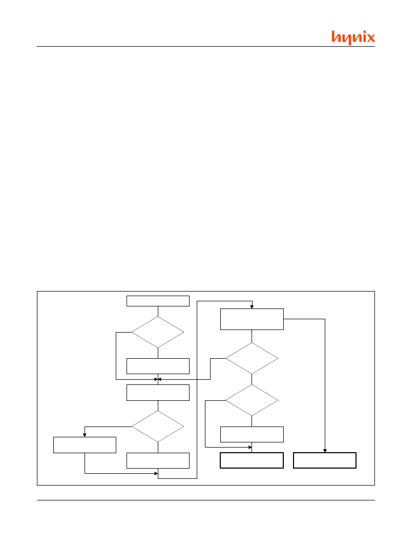
Figure 6 illustrates the programming operation.
Unlock Bypass Command Sequence
Unlock bypass provides a faster method than the
normal Program Command for the host system to
program the array. As shown in Table 9, the Un-
lock Bypass Command sequence consists of two
unlock write cycles followed by a third write cycle
containing the unlock bypass command, 0x20.
The device then enters Unlock Bypass mode. In
this mode, a two-cycle Unlock Bypass Program
Command sequence is used instead of the stan-
dard four-cycle sequence to invoke a program-
ming operation. The first cycle in this sequence
contains the unlock bypass program command,
0xA0, and the second cycle specifies the program
address and data, thus eliminating the initial two
unlock cycles required in the standard Program
Command sequence. Additional data is pro-
grammed in the same manner. The unlock by-
pass mode does not affect normal read operations.
During the unlock bypass mode, only the Unlock
Bypass Program and the Unlock Bypass Reset
commands are valid. To exit the Unlock Bypass
mode, the host must issue the two-cycle Unlock
Bypass Reset command sequence shown in Table
9.
Figure 6 illustrates the procedures for the normal
and unlock bypass program operations.
The device automatically enters the unlock bypass
mode when it is placed in Accelerate mode via
the ACC pin.
START
Enable Fast
Programming
Issue UNLOCK BYPASS
Command
YES
NO
Unlock Bypass
Mode
Issue UNLOCK BYPASS
PROGRAM Command
Issue NORMAL PROGRAM
Command
Check Programming Status
(See Write Operation Status
Section)
YES
NO
Last Word/Byte
Done
YES
NO
Setup Next Address/Data for
Program Operation
YES
NO
Unlock Bypass
Mode
Issue UNLOCK BYPASS
RESET Command
PROGRAMMING
COMPLETE
GO TO ERROR
RECOVERY PROCEDURE
DQ[5] Error Exit
Programming Verified
Figure 6. Normal and Unlock Bypass Programming Procedures
相关PDF资料 |
PDF描述 |
|---|---|
| HY29LV320BF-70I | 32 Mbit (2M x 16) Low Voltage Flash Memory |
| HY29LV320BF-80I | ECONOLINE: RKZ - Safety standards and approvals: EN 60950 certified, rated for 250VAC (LVD test report)- Custom Solutions Available- 3kVDC & 4kVDC Isolation- UL94V-0 Package Material- Power Sharing on Output- Efficiency to 84% |
| HY29LV320BF-90I | 32 Mbit (2M x 16) Low Voltage Flash Memory |
| HY29LV320BT-70 | 32 Mbit (2M x 16) Low Voltage Flash Memory |
| HY29LV320BF-90 | 32 Mbit (2M x 16) Low Voltage Flash Memory |
相关代理商/技术参数 |
参数描述 |
|---|---|
| HY29LV320BF-80I | 制造商:HYNIX 制造商全称:Hynix Semiconductor 功能描述:32 Mbit (2M x 16) Low Voltage Flash Memory |
| HY29LV320BF-90 | 制造商:HYNIX 制造商全称:Hynix Semiconductor 功能描述:32 Mbit (2M x 16) Low Voltage Flash Memory |
| HY29LV320BF-90I | 制造商:HYNIX 制造商全称:Hynix Semiconductor 功能描述:32 Mbit (2M x 16) Low Voltage Flash Memory |
| HY29LV320BT-12 | 制造商:HYNIX 制造商全称:Hynix Semiconductor 功能描述:32 Mbit (2M x 16) Low Voltage Flash Memory |
| HY29LV320BT-12I | 制造商:HYNIX 制造商全称:Hynix Semiconductor 功能描述:32 Mbit (2M x 16) Low Voltage Flash Memory |
发布紧急采购,3分钟左右您将得到回复。