- 您现在的位置:买卖IC网 > PDF目录384464 > HY29LV320BT-90 (HYNIX SEMICONDUCTOR INC) 32 Mbit (2M x 16) Low Voltage Flash Memory PDF资料下载
参数资料
| 型号: | HY29LV320BT-90 |
| 厂商: | HYNIX SEMICONDUCTOR INC |
| 元件分类: | DRAM |
| 英文描述: | 32 Mbit (2M x 16) Low Voltage Flash Memory |
| 中文描述: | 2M X 16 FLASH 3V PROM, 90 ns, PDSO48 |
| 封装: | TSOP-48 |
| 文件页数: | 28/44页 |
| 文件大小: | 323K |
| 代理商: | HY29LV320BT-90 |
第1页第2页第3页第4页第5页第6页第7页第8页第9页第10页第11页第12页第13页第14页第15页第16页第17页第18页第19页第20页第21页第22页第23页第24页第25页第26页第27页当前第28页第29页第30页第31页第32页第33页第34页第35页第36页第37页第38页第39页第40页第41页第42页第43页第44页
28
r1.3/May 02
HY29LV320
ABSOLUTE MAXIMUM RATINGS
4
l
o
b
m
y
S
T
G
T
S
a
S
T
S
A
B
m
A
a
V
r
e
m
a
r
a
P
e
1
1
u
V
o
5
o
5
t
n
C
o
C
o
U
e
p
m
e
p
m
e
T
n
P
n
o
V
C
C
O
,
A
r
h
O
l
A
c
C
t
h
S
e
T
e
t
e
g
g
0
5
5
2
+
+
6
6
d
e
p
A
r
w
o
P
o
e
h
w
p
s
e
R
e
V
2
N
I
V
h
w
S
S
:
1
#
T
E
S
E
R
,
C
C
A
/
P
s
e
C
W
n
P
t
,
E
2
1
0
+
5
1
+
+
0
0
o
o
V
(
2
5
5
o
5
C
C
)
V
V
V
I
S
O
t
t
p
O
3
A
m
Notes:
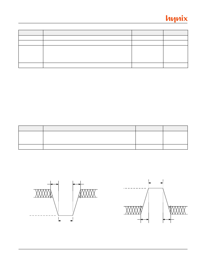
1. Minimum DC voltage on input or I/O pins is
–
0.5 V. During voltage transitions, input or I/O pins may undershoot V
to
-2.0V for periods of up to 20 ns. See Figure 11. Maximum DC voltage on input or I/O pins is V
+ 0.5 V. During voltage
transitions, input or I/O pins may overshoot to V
+2.0 V for periods up to 20 ns. See Figure 12.
2. Minimum DC input voltage on pins A[9], WP#/ACC, OE#, and RESET# is -0.5 V. During voltage transitions, A[9], WP#/
ACC, OE#, and RESET# may undershoot V
to
–
2.0 V for periods of up to 20 ns. See Figure 11. Maximum DC input
voltage on pins A[9], WP#/ACC, OE# and RESET# is +12.5 V which may overshoot to 14.0 V for periods up to 20 ns.
3. No more than one output at a time may be shorted to V
. Duration of the short circuit should be less than one second.
4. Stresses above those listed under
“
Absolute Maximum Ratings
”
may cause permanent damage to the device. This is a
stress rating only; functional operation of the device at these or any other conditions above those indicated in the
operational sections of this data sheet is not implied. Exposure of the device to absolute maximum rating conditions for
extended periods may affect device reliability.
RECOMMENDED OPERATING CONDITIONS
1
l
o
b
m
y
S
r
e
m
a
r
a
P
:
p
m
e
p
m
e
T
e
p
m
e
g
a
V
e
u
V
t
n
U
T
A
e
T
g
n
p
O
m
m
o
C
l
u
d
n
u
S
g
t
e
m
A
s
e
c
e
s
e
D
l
c
e
D
e
T
0
8
2
7
+
+
o
o
0
e
N
0
5
4
C
o
C
o
V
V
C
C
y
p
n
p
O
Notes:
1. Recommended Operating Conditions define those limits between which the functionality of the device is guaranteed.
2. See Valid Combinations table, page 43.
2.0 V
V
CC
+ 0.5 V
V
CC
+ 2.0 V
20 ns
20 ns
20 ns
Figure 11. Maximum Undershoot Waveform
Figure 12. Maximum Overshoot Waveform
0.8 V
- 0.5 V
- 2.0 V
20 ns
20 ns
20 ns
相关PDF资料 |
PDF描述 |
|---|---|
| HY29LV320TF-70 | 32 Mbit (2M x 16) Low Voltage Flash Memory |
| HY29LV320TF-80 | 32 Mbit (2M x 16) Low Voltage Flash Memory |
| HY29LV320BF-80 | 32 Mbit (2M x 16) Low Voltage Flash Memory |
| HY29LV320BF-70I | 32 Mbit (2M x 16) Low Voltage Flash Memory |
| HY29LV320BF-80I | ECONOLINE: RKZ - Safety standards and approvals: EN 60950 certified, rated for 250VAC (LVD test report)- Custom Solutions Available- 3kVDC & 4kVDC Isolation- UL94V-0 Package Material- Power Sharing on Output- Efficiency to 84% |
相关代理商/技术参数 |
参数描述 |
|---|---|
| HY29LV320BT-90I | 制造商:HYNIX 制造商全称:Hynix Semiconductor 功能描述:32 Mbit (2M x 16) Low Voltage Flash Memory |
| HY29LV320T | 制造商:HYNIX 制造商全称:Hynix Semiconductor 功能描述:32 Mbit (2M x 16) Low Voltage Flash Memory |
| HY29LV320TF-12 | 制造商:HYNIX 制造商全称:Hynix Semiconductor 功能描述:32 Mbit (2M x 16) Low Voltage Flash Memory |
| HY29LV320TF-12I | 制造商:HYNIX 制造商全称:Hynix Semiconductor 功能描述:32 Mbit (2M x 16) Low Voltage Flash Memory |
| HY29LV320TF-70 | 制造商:HYNIX 制造商全称:Hynix Semiconductor 功能描述:32 Mbit (2M x 16) Low Voltage Flash Memory |
发布紧急采购,3分钟左右您将得到回复。