- 您现在的位置:买卖IC网 > PDF目录67681 > IBM25405GP-3BA200C2 RISC PROCESSOR, PBGA456 PDF资料下载
参数资料
| 型号: | IBM25405GP-3BA200C2 |
| 元件分类: | 微控制器/微处理器 |
| 英文描述: | RISC PROCESSOR, PBGA456 |
| 封装: | PLASTIC, BGA-456 |
| 文件页数: | 38/48页 |
| 文件大小: | 649K |
| 代理商: | IBM25405GP-3BA200C2 |
第1页第2页第3页第4页第5页第6页第7页第8页第9页第10页第11页第12页第13页第14页第15页第16页第17页第18页第19页第20页第21页第22页第23页第24页第25页第26页第27页第28页第29页第30页第31页第32页第33页第34页第35页第36页第37页当前第38页第39页第40页第41页第42页第43页第44页第45页第46页第47页第48页
PowerPC 405GP Embedded Controller
Advance Information
Data Sheet
galdsh5f
06/15/99 Preliminary
IBM Corporation. All rights reserved.
Use is further subject to the provisions at the end of this document.
Page 43 of 48
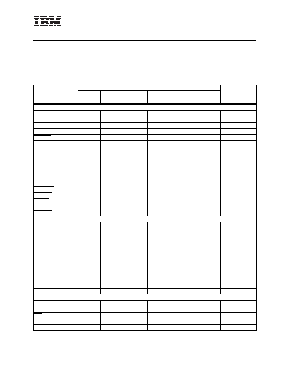
I/O Specications (Part 1 of 3)
Notes:
1. SDRAM command interface is a two-cycle path (first driven in cycle 1 and then sampled at SDRAMs in cycle 2)
2. Output timings are actually relative to a rising edge of the internal PLB bus clock, which is always an integer multiple of
SysClk. The on chip PLL maintains this internal clock such that it is rising edge aligned with SysClk. For this reason all
SDRAM output timings are shown relative to SysClk.
3. Asynchronous PCI timings at 66MHz maximum
Signal
Input (ns)
Output (ns)
Output Current (mA)
Clock
Notes
Setup Time
(minimum)
Hold Time
(minimum)
Valid Delay
(maximum)
50pF load
Hold Time
(minimum)
50 pF load
I/O H
(maximum)
I/O L
(minimum)
PCI Interface
PCIAD0:31
3
0
6
1
12.3
15.5
PCIClk
3
PCIC0:3[BE0:3]
3
0
6
1
12.3
15.5
PCIClk
3
PCIClk
dc
n/a
async
PCIDevSel
3
0
6
1
12.3
15.5
PCIClk
3
PCIFrame
3
0
6
1
12.3
15.5
PCIClk
3
PCIGnt0[Req]
PCIGnt1:5
n/a
6
1
12.3
15.5
PCIClk
3
PCIIDSel
3
0
6
1
n/a
PCIClk
3
PCIINT[PerWE]
n/a
dc
12.3
15.5
PCIClk
async
PCIIRDY
3
0
6
1
12.3
15.5
PCIClk
3
PCIParity
3
0
6
1
12.3
15.5
PCIClk
3
PCIPErr
3
0
6
1
12.3
15.5
PCIClk
3
PCIReq0[Gnt]
PCIReq1:5
5
0
n/a
PCIClk
3
PCIReset
n/a
12.3
15.5
PCIClk
PCISErr
n/a
12.3
15.5
PCIClk
PCIStop
3
0
6
1
12.3
15.5
PCIClk
3
PCITRDY
3
0
6
1
12.3
15.5
PCIClk
3
Ethernet Interface
EMCMDClk
n/a
settable
2
9
6
async
EMCMDIO[PHYMDIO]
n/a
36
2
9
6
PHYTX
EMCTxD0:3
n/a
20
2
9
6
PHYTX
EMCTxEn
n/a
20
2
9
6
PHYTX
EMCTxErr
n/a
20
2
9
6
PHYTX
PHYCol
9
6
async
PHYCrS
9
6
async
PHYRxClk
n/a
async
PHYRxD0:3
4
1
n/a
9
6
PHYRxDV
4
1
n/a
9
6
PHYRxErr
4
1
n/a
9
6
PHYTxClk
n/a
async
SDRAM Interface
BA0:1
n/a
8.25
2
19
12
SysClk
1, 2
BankSel0:3
n/a
7
1.8
19
12
SysClk
2
CAS
n/a
8.25
2
19
12
SysClk
1, 2
ClkEn0:1
n/a
6.8
1.6
40
25
SysClk
2
DQM0:3
n/a
7
1.8
19
12
SysClk
2
相关PDF资料 |
PDF描述 |
|---|---|
| IBM25EMPPC603EFG-100 | 32-BIT, 100 MHz, RISC PROCESSOR, PQFP240 |
| IBM25EMPPC603EBG-100 | 32-BIT, 100 MHz, RISC PROCESSOR, CBGA255 |
| IBM25EMPPC740LDBC4000 | 32-BIT, 400 MHz, RISC PROCESSOR, CBGA255 |
| IBM25EMPPC750LCBF3330 | 32-BIT, 333 MHz, RISC PROCESSOR, CBGA360 |
| IBM25EMPPC740LFBF4000 | 32-BIT, 400 MHz, RISC PROCESSOR, CBGA255 |
相关代理商/技术参数 |
参数描述 |
|---|---|
| IBM25C710AB3A100 | 制造商:未知厂家 制造商全称:未知厂家 功能描述:Controller Miscellaneous - Datasheet Reference |
| IBM25CPC700BB3B66 | 制造商:未知厂家 制造商全称:未知厂家 功能描述:Peripheral (Multifunction) Controller |
| IBM25CPC700BB3B83 | 制造商:未知厂家 制造商全称:未知厂家 功能描述:Peripheral (Multifunction) Controller |
| IBM25CPC700CB3A83 | 制造商:IBM 功能描述: |
| IBM25CPC700CB3B66 | 制造商:未知厂家 制造商全称:未知厂家 功能描述:Peripheral (Multifunction) Controller |
发布紧急采购,3分钟左右您将得到回复。