- 您现在的位置:买卖IC网 > PDF目录67683 > IBM25PPC750FX-GB0112T 32-BIT, 600 MHz, RISC PROCESSOR, CBGA292 PDF资料下载
参数资料
| 型号: | IBM25PPC750FX-GB0112T |
| 元件分类: | 微控制器/微处理器 |
| 英文描述: | 32-BIT, 600 MHz, RISC PROCESSOR, CBGA292 |
| 封装: | 21 X 21 MM, 1 MM PITCH, CERAMIC, BGA-292 |
| 文件页数: | 7/62页 |
| 文件大小: | 452K |
| 代理商: | IBM25PPC750FX-GB0112T |
第1页第2页第3页第4页第5页第6页当前第7页第8页第9页第10页第11页第12页第13页第14页第15页第16页第17页第18页第19页第20页第21页第22页第23页第24页第25页第26页第27页第28页第29页第30页第31页第32页第33页第34页第35页第36页第37页第38页第39页第40页第41页第42页第43页第44页第45页第46页第47页第48页第49页第50页第51页第52页第53页第54页第55页第56页第57页第58页第59页第60页第61页第62页
DD 2.X
Preliminary
PowerPC 750FX RISC Microprocessor
Body_750FX_DS_DD2.X.fm.2.0
June 9, 2003
3. Electrical and Thermal Characteristics
Page 13 of 63
3.2 Clock AC Specications
Table 3-6 provides the clock AC timing specifications as defined in Figure 3-1.
Table 3-6. Clock AC Timing Specications (See Table 3-2 on page 10 for recommended operating
conditions1,6)
Num
(Timing Reference)
Characteristic
Value
Unit
Notes
Min.
Max.
Processor frequency
400
800
MHz
7
SYSCLK frequency
20
200
MHz
1, 6
1
SYSCLK cycle time
5.0
50
ns
2, 3
SYSCLK rise and fall slew rate
1.0
—
V/ns
3
4
SYSCLK duty cycle measured at 0.8V
25
75
%
3
VMSYSCLK
Measurement Reference Voltage for SYSCLK (all I/O voltages)
0.65
V
SYSCLK cycle-to-cycle jitter
–
±150
ps
4, 3
Internal PLL relock time
–
100
s5
Notes:
1. Caution: The SYSCLK frequency and the PLL_CFG[0:4] settings must be chosen such that the resulting SYSCLK (bus)
frequency, CPU (core) frequency, and PLL frequency do not exceed their respective maximum or minimum operating frequencies.
Refer to the PLL_CFG[0:4] signal description in Table 5-2, “750FX Microprocessor PLL Configuration” on page 33 for valid
PLL_CFG[0:4] settings.
2. The SYSCLK slew rate applies between 0.4V and 1.0V.
3. Timing is guaranteed by design and characterization, and is not tested.
4. See Section 3.3 Spread Spectrum Clock Generator (SSCG) on page 14 for long term jitter.
5. Relock timing is guaranteed by design and characterization, and is not tested. PLL-relock time is the maximum amount of time
required for PLL lock after a stable VDD and SYSCLK are reached during the power-on reset sequence. This specication also
applies when the PLL has been disabled and subsequently re-enabled during sleep mode. Also note that HRESET must be held
asserted for a minimum of 255 bus clocks after the PLL-relock time during the power-on reset sequence.
6. This is a statement of the capability of the 750FX I/O circuitry. Not all systems can run at the maximum SYSCLK frequency. Con-
tact IBM PowerPC Application Engineering for more information on high-speed bus design.
7. Lower voltage/frequency operation: For additional information, see 750FX Datasheet Supplement for DD2.X Revisions.
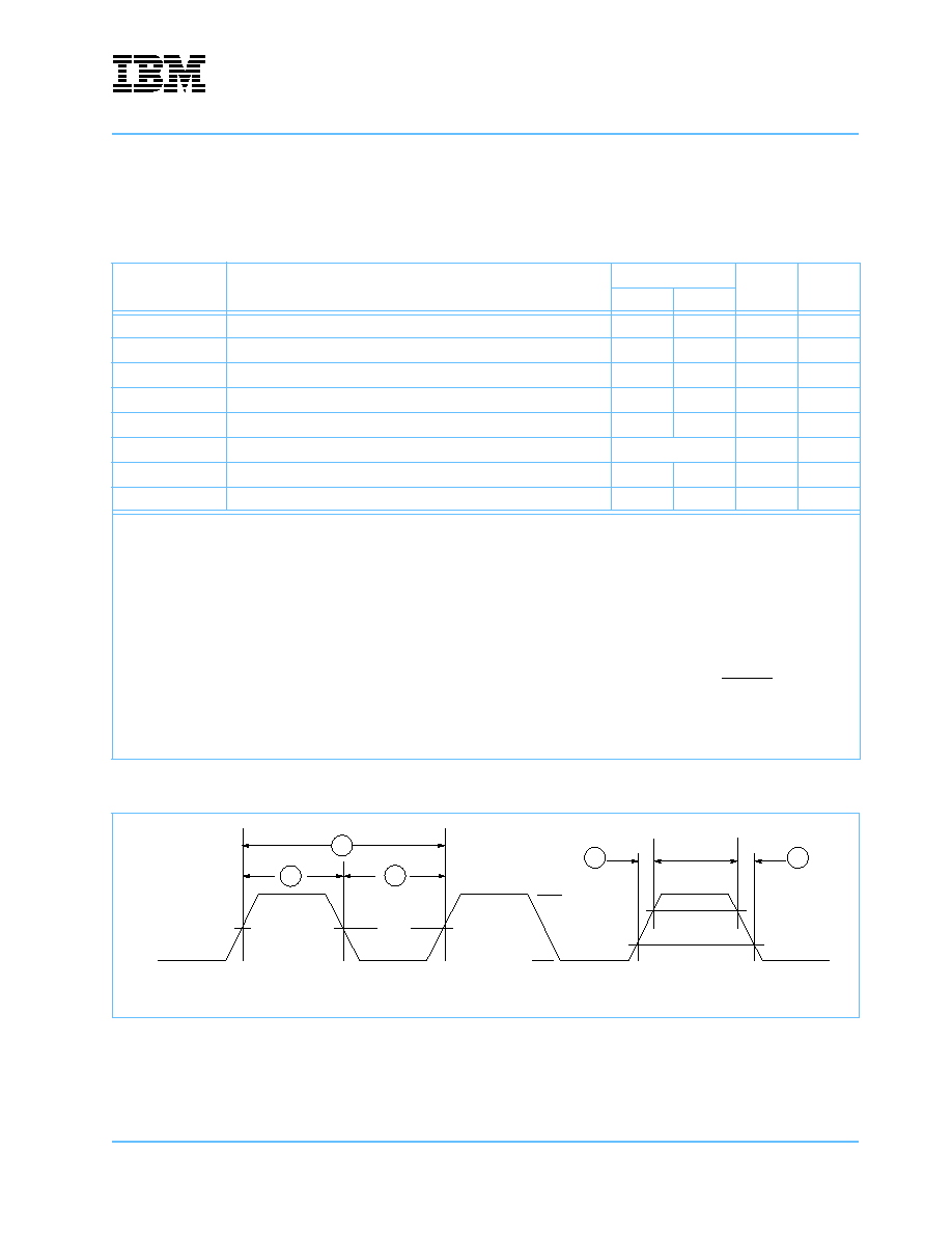
Figure 3-1. SYSCLK Input Timing Diagram
VM
CV
IL
CV
IH
1
2
4
3
4
SYSCLK
VMSYSCLK - Midpoint Voltage for SYSCLK
相关PDF资料 |
PDF描述 |
|---|---|
| IBM25PPC750FX-DB0513T | 32-BIT, 700 MHz, RISC PROCESSOR, CBGA292 |
| IBM25PPC750FX-FB0533T | 32-BIT, 700 MHz, RISC PROCESSOR, CBGA292 |
| IBM25PPC750FX-FB0112T | 32-BIT, 600 MHz, RISC PROCESSOR, CBGA292 |
| IBM25PPC750FX-GB0123T | 32-BIT, 600 MHz, RISC PROCESSOR, CBGA292 |
| IBM25PPC750FX-EB0122T | 32-BIT, 600 MHz, RISC PROCESSOR, CBGA292 |
相关代理商/技术参数 |
参数描述 |
|---|---|
| IBM25PPC750FX-GB0122V | 制造商:IBM 功能描述:MPU 750XX RISC 32BIT - Trays |
| IBM25PPC750FX-GB0132T | 制造商:IC'S/TRANSISTORS/DIO 功能描述: 制造商:IC'S/TRANSISTORS/DIODES 功能描述: |
| IBM25PPC750FX-GB0132V | 制造商:IBM 功能描述:MPU 750XX RISC 32BIT - Trays |
| IBM25PPC750FX-GB0133V | 制造商:IBM 功能描述:MPU 750XX RISC 32BIT - Trays |
| IBM25PPC750FX-GB0532V | 制造商:IBM 功能描述:MPU 750XX RISC 32BIT - Trays |
发布紧急采购,3分钟左右您将得到回复。