- 您现在的位置:买卖IC网 > PDF目录136444 > IBM25PPC750L-FB0A400W 32-BIT, 400 MHz, RISC PROCESSOR, CBGA360 PDF资料下载
参数资料
| 型号: | IBM25PPC750L-FB0A400W |
| 元件分类: | 微控制器/微处理器 |
| 英文描述: | 32-BIT, 400 MHz, RISC PROCESSOR, CBGA360 |
| 封装: | 25 X 25 MM, 1.27 MM PITCH, CERAMIC, BGA-360 |
| 文件页数: | 7/46页 |
| 文件大小: | 610K |
| 代理商: | IBM25PPC750L-FB0A400W |
第1页第2页第3页第4页第5页第6页当前第7页第8页第9页第10页第11页第12页第13页第14页第15页第16页第17页第18页第19页第20页第21页第22页第23页第24页第25页第26页第27页第28页第29页第30页第31页第32页第33页第34页第35页第36页第37页第38页第39页第40页第41页第42页第43页第44页第45页第46页
9/30/99
Version 2.0
Datasheet
Page 11
PowerPC 750 SCM RISC Microprocessor
Preliminary Copy
PID8p-750
60x Bus Input AC Specications
The following table provides the 60X bus input AC timing specifications for the PID8p-750 as defined in
Figure 3 and Figure 4. Input timing specifications for the L2 bus are provided in Section, “L2 Bus Input AC
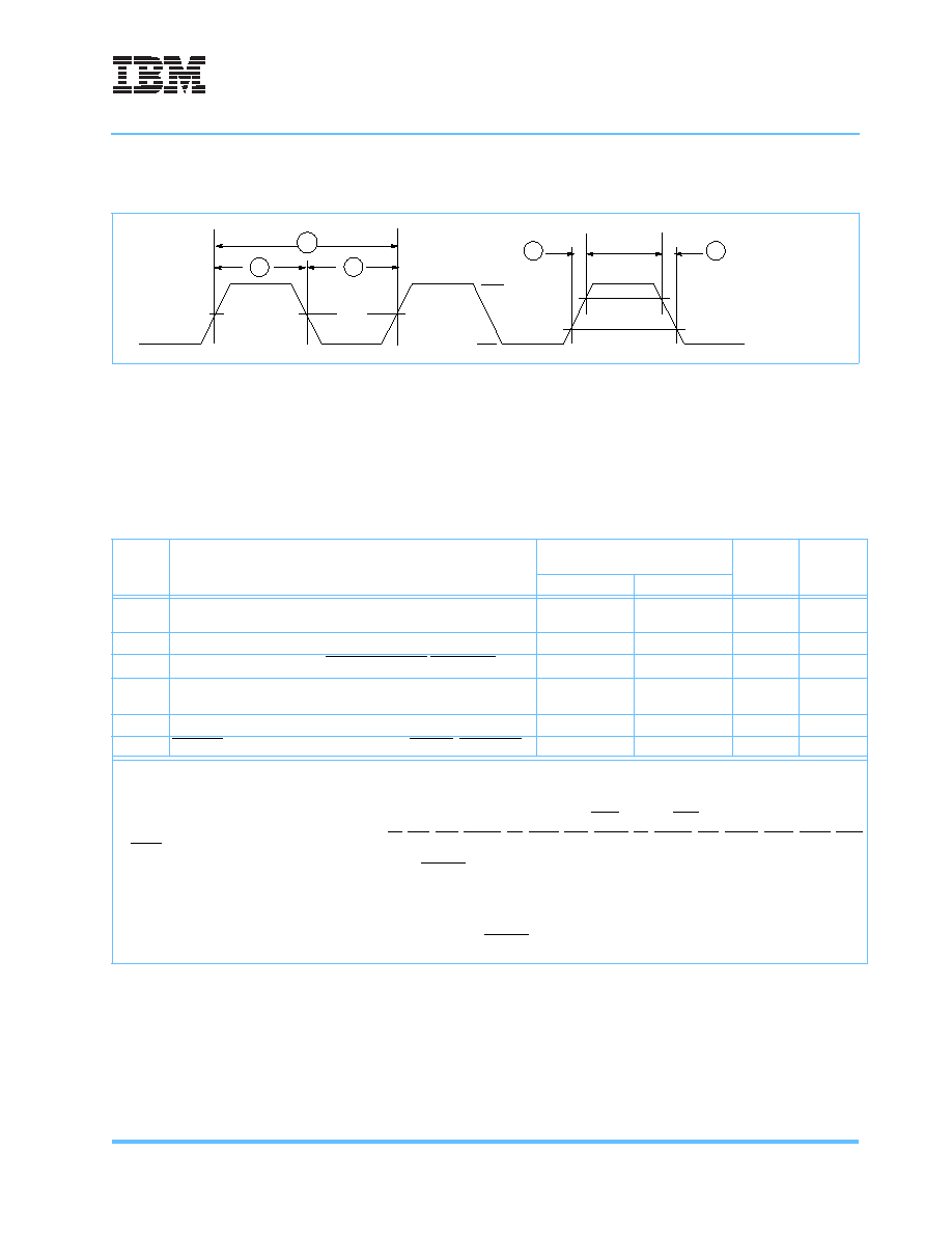
Figure 2. SYSCLK Input Timing Diagram
60X Bus Input Timing Specications1
See Table “Recommended Operating Conditions1,2,3,” on page 6, for operating conditions.
Num
Characteristic
300,333, 350, 366,
375, 400, 433, 450, 466, 500 MHz
Unit
Notes
Minimum
Maximum
10a
Address/Data/Transfer Attribute Inputs Valid to SYSCLK (Input
Setup)
2.5
—
ns
2
10b
All Other Inputs Valid to SYSCLK (Input Setup)
2.5
—
ns
3
10c
Mode Select Input Setup to HRESET (DRTRY,TLBISYNC)
8
—
tsysclk
4,5,6,7
11a
SYSCLK to Address/Data/Transfer Attribute Inputs Invalid (Input
Hold)
0.6
—
ns
2
11b
SYSCLK to All Other Inputs Invalid (Input Hold)
0.6
—
ns
3
11c
HRESET to mode select input hold
(DRTRY, TLBISYNC)
0
—
ns
4,6,7
Note:
1. Input specifications are measured from the midpoint voltage of the signal in question to the midpoint voltage of the rising edge of the input SYSCLK. Input
and output timings are measured at the pin (see Figure 3) Midpoint voltage (VM) is 1.4v for OVdd in 3.3v mode and OVDD/2 for all other I/O modes
2. Address/Data Transfer Attribute inputs are composed of the following–A[0-31], AP[0-3], TT[0-4],TBST, TSIZ[0-2], GBL, DH[0-31), DL[0-31], DP[0-7].
3. All other signal inputs are composed of the following–TS, ABB, DBB, ARTRY, BG, AACK, DBG, DBWO, TA, DRTRY, TEA, DBDIS, TBEN, QACK, TLBI-
SYNC.
4. The setup and hold time is with respect to the rising edge of HRESET (see Figure 4).
5. tSYSCLK, is the period of the external clock (SYSCLK) in nanoseconds (ns). The numbers given in the table must be multiplied by the period of SYSCLK to
compute the actual time duration (in ns) of the parameter in question.
6. These values are guaranteed by design, and are not tested.
7. This specification is for configuration mode select only. Also note that the HRESET must be held asserted for a minimum of 255 bus clocks after the
PLL re-lock time during the power-on reset sequence.
VM
CV
IL
CV
IH
1
2
4
3
4
SYSCLK
(Midpoint
Voltage)
相关PDF资料 |
PDF描述 |
|---|---|
| IBM25PPC750L-FB0A466W | 32-BIT, 466 MHz, RISC PROCESSOR, CBGA360 |
| IBM25PPC750GXEAR5H43T | 32-BIT, 933 MHz, RISC PROCESSOR, CBGA292 |
| IBM25PPC750GXEBB6572T | 32-BIT, 1000 MHz, RISC PROCESSOR, CBGA292 |
| ISL8705IBZ | DSP-ADDRESS SEQUENCER, PDSO14 |
| ICS932S208DG | 400 MHz, PROC SPECIFIC CLOCK GENERATOR, PDSO56 |
相关代理商/技术参数 |
参数描述 |
|---|---|
| IBM25PPC750L-FB0B300W | 制造商:未知厂家 制造商全称:未知厂家 功能描述:32-Bit Microprocessor |
| IBM25PPC750L-FB0B333W | 制造商:未知厂家 制造商全称:未知厂家 功能描述:32-Bit Microprocessor |
| IBM25PPC750L-FB0B350W | 制造商:未知厂家 制造商全称:未知厂家 功能描述:32-Bit Microprocessor |
| IBM25PPC750L-FB0B366W | 制造商:未知厂家 制造商全称:未知厂家 功能描述:32-Bit Microprocessor |
| IBM25PPC750L-FB0B375W | 制造商:未知厂家 制造商全称:未知厂家 功能描述:32-Bit Microprocessor |
发布紧急采购,3分钟左右您将得到回复。