参数资料
| 型号: | ICL7660SIPA |
| 厂商: | Intersil |
| 文件页数: | 8/13页 |
| 文件大小: | 0K |
| 描述: | IC REG SWITCHED CAP DBL INV 8DIP |
| 标准包装: | 1,000 |
| 类型: | 切换式电容器(充电泵),倍增器,反相 |
| 输出类型: | 可调式 |
| 输出数: | 1 |
| 输出电压: | -1.5 V ~ -12 V,±3 V ~ ±24 V |
| 输入电压: | 1.5 V ~ 12 V |
| 频率 - 开关: | 10kHz,35kHz |
| 电流 - 输出: | 45mA |
| 同步整流器: | 无 |
| 工作温度: | -40°C ~ 85°C |
| 安装类型: | 通孔 |
| 封装/外壳: | 8-DIP(0.300",7.62mm) |
| 包装: | 管件 |
| 供应商设备封装: | 8-PDIP |
�� �
�
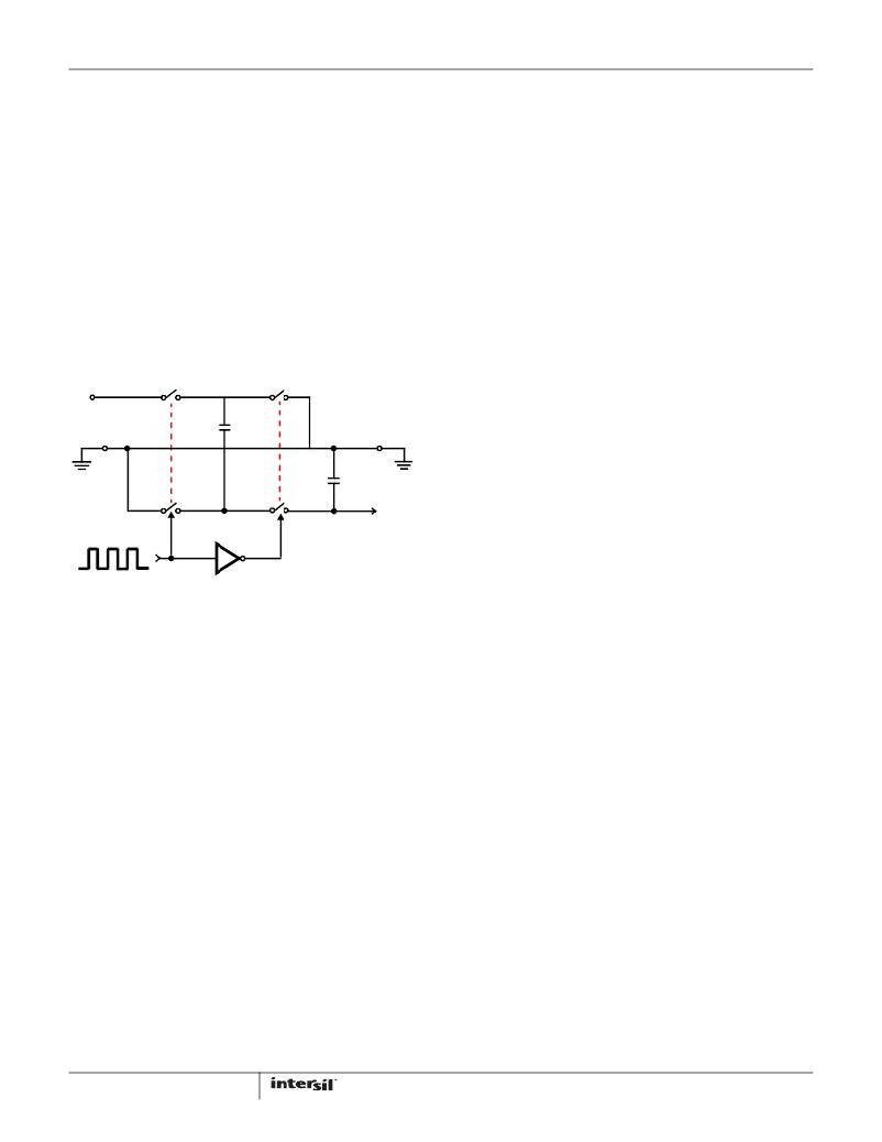
�ICL7660S,� ICL7660A�
�Detailed� Description�
�The� ICL7660S� and� ICL7660A� contain� all� the� necessary�
�circuitry� to� complete� a� negative� voltage� converter,� with� the�
�exception� of� two� external� capacitors,� which� may� be�
�inexpensive� 10μF� polarized� electrolytic� types.� The� mode� of�
�operation� of� the� device� may� best� be� understood� by�
�considering� Figure� 14,� which� shows� an� idealized� negative�
�voltage� converter.� Capacitor� C� 1� is� charged� to� a� voltage,� V+,�
�for� the� half� cycle,� when� switches� S� 1� and� S� 3� are� closed.�
�(Note:� Switches� S� 2� and� S� 4� are� open� during� this� half� cycle).�
�During� the� second� half� cycle� of� operation,� switches� S� 2� and�
�S� 4� are� closed,� with� S� 1� and� S� 3� open,� thereby� shifting�
�capacitor� C� 1� to� C� 2� such� that� the� voltage� on� C� 2� is� exactly� V+,�
�assuming� ideal� switches� and� no� load� on� C� 2� .� The� ICL7660S�
�and� ICL7660A� approach� this� ideal� situation� more� closely�
�than� existing� non-mechanical� circuits.�
�Theoretical� Power� Efficiency�
�Considerations�
�In� theory,� a� voltage� converter� can� approach� 100%� efficiency�
�if� certain� conditions� are� met:�
�1.� The� drive� circuitry� consumes� minimal� power.�
�2.� The� output� switches� have� extremely� low� ON� resistance�
�and� virtually� no� offset.�
�3.� The� impedance� of� the� pump� and� reservoir� capacitors� are�
�negligible� at� the� pump� frequency.�
�The� ICL7660S� and� ICL7660A� approach� these� conditions� for�
�negative� voltage� conversion� if� large� values� of� C� 1� and� C� 2� are�
�used.� ENERGY� IS� LOST� ONLY� IN� THE� TRANSFER� OF�
�CHARGE� BETWEEN� CAPACITORS� IF� A� CHANGE� IN�
�VOLTAGE� OCCURS� .� The� energy� lost� is� defined� as� shown� in�
�Equation� 1:�
�E� =� ---� C� 1� (� V� 1� 2� –� V� 2� 2� )�
�V� IN�
�8�
�S� 1�
�2�
�S� 2�
�1�
�2�
�(EQ.� 1)�
�3�
�C� 1�
�3�
�where� V� 1� and� V� 2� are� the� voltages� on� C� 1� during� the� pump�
�and� transfer� cycles.� If� the� impedances� of� C� 1� and� C� 2� are�
�relatively� high� at� the� pump� frequency� (see� Figure� 14)�
�S� 3�
�4�
�S� 4�
�C� 2�
�5�
�V� OUT� =� -V� IN�
�compared� to� the� value� of� R� L� ,� there� will� be� a� substantial�
�difference� in� the� voltages,� V� 1� and� V� 2� .� Therefore� it� is� not� only�
�desirable� to� make� C� 2� as� large� as� possible� to� eliminate� output�
�voltage� ripple,� but� also� to� employ� a� correspondingly� large�
�7�
�FIGURE� 14.� IDEALIZED� NEGATIVE� VOLTAGE� CONVERTER�
�In� the� ICL7660S� and� ICL7660A,� the� four� switches� of�
�Figure� 14� are� MOS� power� switches;� S� 1� is� a� P-Channel�
�device;� and� S� 2� ,� S� 3� and� S� 4� are� N-Channel� devices.� The� main�
�difficulty� with� this� approach� is� that� in� integrating� the� switches,�
�the� substrates� of� S� 3� and� S� 4� must� always� remain� reverse�
�biased� with� respect� to� their� sources,� but� not� so� much� as� to�
�degrade� their� “ON”� resistances.� In� addition,� at� circuit� start-�
�up,� and� under� output� short� circuit� conditions� (V� OUT� =� V+),�
�the� output� voltage� must� be� sensed� and� the� substrate� bias�
�adjusted� accordingly.� Failure� to� accomplish� this� would� result�
�in� high� power� losses� and� probable� device� latch-up.�
�This� problem� is� eliminated� in� the� ICL7660S� and� ICL7660A� by�
�a� logic� network� that� senses� the� output� voltage� (V� OUT� )�
�together� with� the� level� translators,� and� switches� the�
�substrates� of� S� 3� and� S� 4� to� the� correct� level� to� maintain�
�necessary� reverse� bias.�
�The� voltage� regulator� portion� of� the� ICL7660S� and�
�ICL7660A� is� an� integral� part� of� the� anti-latchup� circuitry;�
�however,� its� inherent� voltage� drop� can� degrade� operation� at�
�low� voltages.� Therefore,� to� improve� low� voltage� operation,�
�the� “LV”� pin� should� be� connected� to� GND,� thus� disabling� the�
�regulator.� For� supply� voltages� greater� than� 3.5V,� the� LV�
�terminal� must� be� left� open� to� ensure� latchup-proof� operation�
�and� to� prevent� device� damage.�
�8�
�value� for� C� 1� in� order� to� achieve� maximum� efficiency� of�
�operation.�
�Do’s� and� Don’ts�
�1.� Do� not� exceed� maximum� supply� voltages.�
�2.� Do� not� connect� LV� terminal� to� GND� for� supply� voltage�
�greater� than� 3.5V.�
�3.� Do� not� short� circuit� the� output� to� V� +� supply� for� supply�
�voltages� above� 5.5V� for� extended� periods;� however,�
�transient� conditions� including� start-up� are� okay.�
�4.� When� using� polarized� capacitors,� the� +� terminal� of� C� 1� must�
�be� connected� to� pin� 2� of� the� ICL7660S� and� ICL7660A,� and�
�the� +� terminal� of� C� 2� must� be� connected� to� GND.�
�5.� If� the� voltage� supply� driving� the� ICL7660S� and� ICL7660A�
�has� a� large� source� impedance� (25� Ω� to� 30� Ω� ),� then� a�
�2.2μF� capacitor� from� pin� 8� to� ground� may� be� required� to�
�limit� the� rate� of� rise� of� input� voltage� to� less� than� 2V/μs.�
�6.� If� the� input� voltage� is� higher� than� 5V� and� it� has� a� rise� rate�
�more� than� 2V/μs,� an� external� Schottky� diode� from� V� OUT�
�to� CAP-� is� needed� to� prevent� latchup� (triggered� by�
�forward� biasing� Q4’s� body� diode)� by� keeping� the� output�
�(pin� 5)� from� going� more� positive� than� CAP-� (pin� 4).�
�7.� User� should� ensure� that� the� output� (pin� 5)� does� not� go�
�more� positive� than� GND� (pin� 3).� Device� latch-up� will�
�occur� under� these� conditions.� To� provide� additional�
�protection,� a� 1N914� or� similar� diode� placed� in� parallel�
�with� C� 2� will� prevent� the� device� from� latching� up� under�
�these� conditions,� when� the� load� on� V� OUT� creates� a� path�
�to� pull� up� V� OUT� before� the� IC� is� active� (anode� pin� 5,�
�cathode� pin� 3).�
�FN3179.7�
�January� 23,� 2013�
�相关PDF资料 |
PDF描述 |
|---|---|
| ICL7662CPA | IC REG SWITCHED CAP DBL INV 8DIP |
| ICL7663ACPA+ | IC REG LDO ADJ 40MA 8-DIP |
| ICL7663SACBAZA | IC REG LDO ADJ 40MA 8SOIC |
| ICL7665ACPA | IC VOLT DETEC DUAL OVR/UND 8-DIP |
| ICL7665SIBA | IC VOLT DETECTOR OVER/UND 8-SOIC |
相关代理商/技术参数 |
参数描述 |
|---|---|
| ICL7660SIPAZ | 功能描述:电荷泵 W/ANNEAL CMOS VAGE CNVRTR IND RoHS:否 制造商:Maxim Integrated 功能:Inverting, Step Up 输出电压:- 1.5 V to - 5.5 V, 3 V to 11 V 输出电流:100 mA 电源电流:1 mA 最大工作温度:+ 70 C 封装 / 箱体:SOIC-8 Narrow 封装:Tube |
| ICL7660SMTV | 制造商:Rochester Electronics LLC 功能描述: |
| ICL7660TV | 制造商:Harris Corporation 功能描述: |
| ICL7661SCBA | 制造商:Rochester Electronics LLC 功能描述:- Bulk |
| ICL7662 WAF | 制造商:Harris Corporation 功能描述: |
发布紧急采购,3分钟左右您将得到回复。