- 您现在的位置:买卖IC网 > PDF目录67685 > ICS2059GI-02 (INTEGRATED DEVICE TECHNOLOGY INC) 27 MHz, VIDEO CLOCK GENERATOR, PDSO16 PDF资料下载
参数资料
| 型号: | ICS2059GI-02 |
| 厂商: | INTEGRATED DEVICE TECHNOLOGY INC |
| 元件分类: | 时钟产生/分配 |
| 英文描述: | 27 MHz, VIDEO CLOCK GENERATOR, PDSO16 |
| 封装: | 0.173 INCH, TSSOP-16 |
| 文件页数: | 5/12页 |
| 文件大小: | 309K |
| 代理商: | ICS2059GI-02 |
Clock Multiplier and Jitter Attenuator
MDS 2059-02 C
2
Revision 031605
Integrated Circuit Systems, Inc.
● 525 Race Street, San Jose, CA 95126 ● tel (408) 297-1201 ● www.icst.com
ICS2059-02
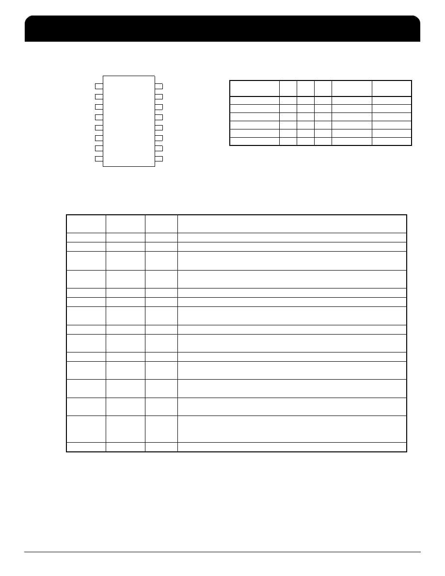
Pin Assignment
Output Frequency Select Table
Note: For SEL input pin programming:
0 = GND, 1 = VDD, M = Floating
Pin Descriptions
13
4
12
5
11
VIN
8
9
10
SEL0
ISET
16
3
VDD
ICLK2
ICLK1
1
X1
VDD
ISEL
X2
14
2
7
GND
SEL1
CLK
GND
15
6
16- pin( 173mil) TSSOP
CHGP
Input
SEL1 SEL0
N
Output Clock
(MHz)
Crystal Used
(MHz)
8 kHz
0
1296
10.368
20.736
8 kHz
0
1
2430
19.44
15.625 kHz
1
0
1728
27
15.734265 kHz
1
1716
27
151.875 kHz
M
0
128
19.44
27 MHz
M
1
27
Pin
Number
Pin
Name
Pin
Type
Pin Description
1
X1
—
Crystal Input. Connect this pin to the specified crystal.
2
VDD
Power
Power Supply. Connect to +3.3 V.
3
VDD
Power
Power Supply. Connect to +3.3 V.
4
VDD
Power
Power Supply. Connect to +3.3 V.
5
VIN
Input
VCXO Control Voltage Input. Connect this pin to CHGP pin and the
external loop filter as shown in this data sheet.
6
GND
Power
Connect to ground.
7
GND
Power
Connect to ground.
8
CHGP
Output
Charge Pump Output. Connect this pin to the external loop filter and to
pin VIN.
9
ISET
—
Charge pump current setting node, connection for setting resistor.
10
SEL1
Input
Output Frequency Selection Pin 1. Determines output frequency as
per table above. Includes mid-level input.
11
CLK
Output
Clock Output.
12
SEL0
Input
Output Frequency Selection Pin 0. Determines output frequency as
per table above. Internal pull-up resistor.
13
ICLK2
Input
Input Clock Connection 2. Connect an input reference clock to this pin.
If unused, connect to ground.
14
ICLK1
Input
Input Clock Connection 1. Connect an input reference clock to this pin.
If unused, connect to ground.
15
ISEL
Input
Input Selection. Used to select which reference input clock is active.
Low input level selects ICLK1, high input level selects ICLK2. Internal
pull-up resistor.
16
X2
—
Crystal Output. Connect this pin to the specified crystal.
ICS2059-02
Clock Multiplier and Jitter Attenuator
TSD
IDT / ICS Clock Multiplier and Jitter Attenuator
ICS2059-02
2
相关PDF资料 |
PDF描述 |
|---|---|
| ICS2304NZGI-1T | 2304 SERIES, LOW SKEW CLOCK DRIVER, 4 TRUE OUTPUT(S), 0 INVERTED OUTPUT(S), PDSO8 |
| ICS2304NZG-1LF | 2304 SERIES, LOW SKEW CLOCK DRIVER, 4 TRUE OUTPUT(S), 0 INVERTED OUTPUT(S), PDSO8 |
| ICS252MI-XXLF | 200 MHz, OTHER CLOCK GENERATOR, PDSO8 |
| ICS252MI-XX | 200 MHz, OTHER CLOCK GENERATOR, PDSO8 |
| ICS252PMI | 200 MHz, OTHER CLOCK GENERATOR, PDSO8 |
相关代理商/技术参数 |
参数描述 |
|---|---|
| ICS2059GI-02LF | 功能描述:IC CLK MULT/JITTER ATTEN 16TSSOP RoHS:是 类别:集成电路 (IC) >> 时钟/计时 - 时钟发生器,PLL,频率合成器 系列:- 标准包装:1,000 系列:- 类型:时钟/频率合成器,扇出分配 PLL:- 输入:- 输出:- 电路数:- 比率 - 输入:输出:- 差分 - 输入:输出:- 频率 - 最大:- 除法器/乘法器:- 电源电压:- 工作温度:- 安装类型:表面贴装 封装/外壳:56-VFQFN 裸露焊盘 供应商设备封装:56-VFQFP-EP(8x8) 包装:带卷 (TR) 其它名称:844S012AKI-01LFT |
| ICS2059GI-02LFT | 功能描述:IC CLK MULT/JITTER ATTEN 16TSSOP RoHS:是 类别:集成电路 (IC) >> 时钟/计时 - 时钟发生器,PLL,频率合成器 系列:- 标准包装:2,000 系列:- 类型:PLL 时钟发生器 PLL:带旁路 输入:LVCMOS,LVPECL 输出:LVCMOS 电路数:1 比率 - 输入:输出:2:11 差分 - 输入:输出:是/无 频率 - 最大:240MHz 除法器/乘法器:是/无 电源电压:3.135 V ~ 3.465 V 工作温度:0°C ~ 70°C 安装类型:表面贴装 封装/外壳:32-LQFP 供应商设备封装:32-TQFP(7x7) 包装:带卷 (TR) |
| ICS2059GI-02T | 功能描述:IC CLK MULT/JITTER ATTEN 16TSSOP RoHS:否 类别:集成电路 (IC) >> 时钟/计时 - 时钟发生器,PLL,频率合成器 系列:- 产品变化通告:Product Discontinuation 04/May/2011 标准包装:96 系列:- 类型:时钟倍频器,零延迟缓冲器 PLL:带旁路 输入:LVTTL 输出:LVTTL 电路数:1 比率 - 输入:输出:1:8 差分 - 输入:输出:无/无 频率 - 最大:133.3MHz 除法器/乘法器:是/无 电源电压:3 V ~ 3.6 V 工作温度:0°C ~ 70°C 安装类型:表面贴装 封装/外壳:16-TSSOP(0.173",4.40mm 宽) 供应商设备封装:16-TSSOP 包装:管件 其它名称:23S08-5HPGG |
| ICS2101M | 制造商:未知厂家 制造商全称:未知厂家 功能描述: |
| ICS2101N | 制造商:未知厂家 制造商全称:未知厂家 功能描述: |
发布紧急采购,3分钟左右您将得到回复。