- 您现在的位置:买卖IC网 > PDF目录65528 > ICS2509CYG-T (INTEGRATED DEVICE TECHNOLOGY INC) 2509 SERIES, PLL BASED CLOCK DRIVER, 9 TRUE OUTPUT(S), 0 INVERTED OUTPUT(S), PDSO24 PDF资料下载
参数资料
| 型号: | ICS2509CYG-T |
| 厂商: | INTEGRATED DEVICE TECHNOLOGY INC |
| 元件分类: | 时钟及定时 |
| 英文描述: | 2509 SERIES, PLL BASED CLOCK DRIVER, 9 TRUE OUTPUT(S), 0 INVERTED OUTPUT(S), PDSO24 |
| 封装: | 4.40 MM, 0.65 MM PITCH, PLASTIC, MO-153, TSSOP-24 |
| 文件页数: | 7/10页 |
| 文件大小: | 304K |
| 代理商: | ICS2509CYG-T |
6
ICS2509C
0008D—03/31/03
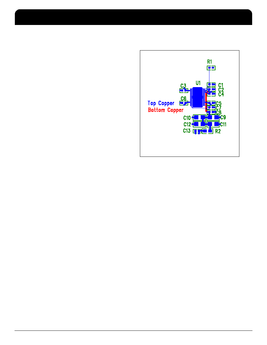
General Layout Precautions:
An ICS2509C is used as an example.
The same rules and methods apply.
1)
Use copper flooded ground on the top signal layer
under the clock buffer The area under U1 in figure 1
on the right is an example. Every ground pin goes to a
ground via. The vias are not visible in figure 1.
2)
Use power vias for power and ground. Vias 20 mil or
larger in diameter have lower high frequency
impedance. Vias for signals may be minimum drill
size.
3)
Make all power and ground traces are as wide as the
via pad for lower inductance.
4)
VAA for pin 23 has a low pass RC filter to decouple
the digital and analog supplies. C9-12 may be replaced
with a single low ESR (0.8 ohm or less) device with
the same total capacitance. R2 may be replaced with a
ferrite bead. The bead should have a DC resistance of
at least 0.5 ohms. 1 ohm is better. It should have an
impedance of at least 300 ohms at 100MHz. 600 ohms
at 100MHz is better.
5)
Notice that ground vias are never shared.
6)
All VCC pins have a decoupling capacitor. Power is
always routed from the plane connection via to the
capacitor pad to the VCC pin on the clock buffer.
7)
Component R1 is located at the clock source.
8)
Component C1, if used, has the effect of adding delay.
9)
Component C7 , if used, has the effect of subtracting
delay. Delaying the FBIn clock will cause the output
clocks to be earlier. A more effective method is to use
the propagation time of a trace between FBOut and
FBIn.
Component Values:
C1,C7= As necessary for delay
adjust
C[6:2]=.01uF
C8,C13=0.1uF
C[12:9]=4.7Uf
R1=10 ohm. Locate at driver
R2=10 ohm.
Figure 1.
ICS2509C
3.3V Phase-Lock Loop Clock Driver
TSD
IDT / ICS 3.3V Phase-Lock Loop Clock Driver
ICS2509C
6
相关PDF资料 |
PDF描述 |
|---|---|
| ICS2509CYGLF-T | PLL BASED CLOCK DRIVER, 9 TRUE OUTPUT(S), 0 INVERTED OUTPUT(S), PDSO24 |
| ICS2509DG | 2509 SERIES, PLL BASED CLOCK DRIVER, 9 TRUE OUTPUT(S), 0 INVERTED OUTPUT(S), PDSO24 |
| ICS2509DGLF | 2509 SERIES, PLL BASED CLOCK DRIVER, 9 TRUE OUTPUT(S), 0 INVERTED OUTPUT(S), PDSO24 |
| ICS2509GLF | 2509 SERIES, PLL BASED CLOCK DRIVER, 9 TRUE OUTPUT(S), 0 INVERTED OUTPUT(S), PDSO24 |
| ICS252PMI | 200 MHz, OTHER CLOCK GENERATOR, PDSO8 |
相关代理商/技术参数 |
参数描述 |
|---|---|
| ICS251 | 制造商:IDT 制造商全称:Integrated Device Technology 功能描述:FIELD PROGRAMMABLE SS VERSACLOCK SYNTHESIZER |
| ICS2510C | 制造商:ICS 制造商全称:ICS 功能描述:3.3V Phase-Lock Loop Clock Driver |
| ICS2510CG | 功能描述:IC CLOCK DVR PLL 3.3V 24-TSSOP RoHS:否 类别:集成电路 (IC) >> 时钟/计时 - 时钟发生器,PLL,频率合成器 系列:- 标准包装:2,000 系列:- 类型:PLL 时钟发生器 PLL:带旁路 输入:LVCMOS,LVPECL 输出:LVCMOS 电路数:1 比率 - 输入:输出:2:11 差分 - 输入:输出:是/无 频率 - 最大:240MHz 除法器/乘法器:是/无 电源电压:3.135 V ~ 3.465 V 工作温度:0°C ~ 70°C 安装类型:表面贴装 封装/外壳:32-LQFP 供应商设备封装:32-TQFP(7x7) 包装:带卷 (TR) |
| ICS2510CGLF | 功能描述:IC CLOCK DVR PLL 3.3V 24-TSSOP RoHS:是 类别:集成电路 (IC) >> 时钟/计时 - 时钟发生器,PLL,频率合成器 系列:- 标准包装:2,000 系列:- 类型:PLL 时钟发生器 PLL:带旁路 输入:LVCMOS,LVPECL 输出:LVCMOS 电路数:1 比率 - 输入:输出:2:11 差分 - 输入:输出:是/无 频率 - 最大:240MHz 除法器/乘法器:是/无 电源电压:3.135 V ~ 3.465 V 工作温度:0°C ~ 70°C 安装类型:表面贴装 封装/外壳:32-LQFP 供应商设备封装:32-TQFP(7x7) 包装:带卷 (TR) |
| ICS2510CGLFT | 功能描述:IC CLOCK DVR PLL 3.3V 24-TSSOP RoHS:是 类别:集成电路 (IC) >> 时钟/计时 - 时钟发生器,PLL,频率合成器 系列:- 标准包装:2,000 系列:- 类型:PLL 时钟发生器 PLL:带旁路 输入:LVCMOS,LVPECL 输出:LVCMOS 电路数:1 比率 - 输入:输出:2:11 差分 - 输入:输出:是/无 频率 - 最大:240MHz 除法器/乘法器:是/无 电源电压:3.135 V ~ 3.465 V 工作温度:0°C ~ 70°C 安装类型:表面贴装 封装/外壳:32-LQFP 供应商设备封装:32-TQFP(7x7) 包装:带卷 (TR) |
发布紧急采购,3分钟左右您将得到回复。