- 您现在的位置:买卖IC网 > PDF目录65528 > ICS2509GLF 2509 SERIES, PLL BASED CLOCK DRIVER, 9 TRUE OUTPUT(S), 0 INVERTED OUTPUT(S), PDSO24 PDF资料下载
参数资料
| 型号: | ICS2509GLF |
| 元件分类: | 时钟及定时 |
| 英文描述: | 2509 SERIES, PLL BASED CLOCK DRIVER, 9 TRUE OUTPUT(S), 0 INVERTED OUTPUT(S), PDSO24 |
| 封装: | 0.173 INCH, TSSOP-24 |
| 文件页数: | 1/7页 |
| 文件大小: | 200K |
| 代理商: | ICS2509GLF |
Integrated
Circuit
Systems, Inc.
General Description
Features
ICS2509
Advance Information
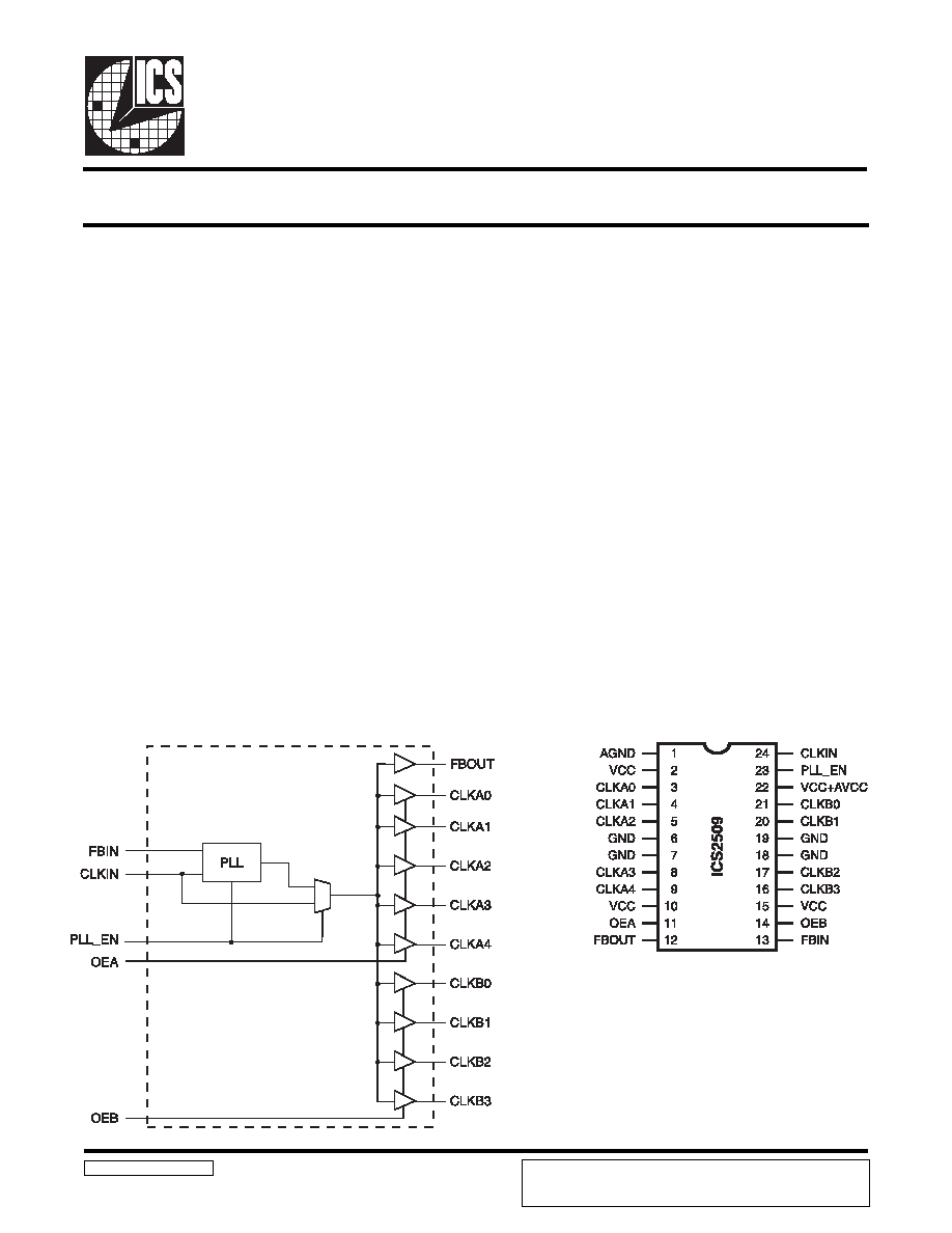
Block Diagram
3.3V Phase-Lock Loop Clock Driver
2509 Rev - 4/20/99
Pin Configuration
24 Pin TSSOP
ADVANCE INFORMATION documents contain information on products
in the formative or design phase development. Characteristic data and
other specifications are design goals. ICS reserves the right to change or
discontinue these products without notice.
The ICS2509 is a high performance, low skew, low jitter
clock driver. It uses a phase lock loop (PLL) technology to
align, in both phase and frequency, the CLKIN signal with
the CLKOUT signal. It is specifically designed for use with
synchronous SDRAMs. The ICS2509 operates at 3.3V VCC
and drive up to nine clock loads.
One bank of five outputs and one bank of four outputs provide
nine low-skew, low-jitter copies of CLKIN. Output signal
duty cycles are adjusted to 50 percent, independent of the
duty cycle at CLKIN. Each bank of outputs can be enabled or
disabled separately via control (OEA and OEB) inputs. When
the OE inputs are high, the outputs align in phase and
frequency with CLKIN; when the OE inputs are low, the
outputs are disabled to the logic low state.
The ICS2509 does not require external RC filter components.
The loop filter for the PLL is include on-chip, minimizing
component count, board space, and cost. The buffer mode
shuts off the PLL and connects the input directly to the
output buffer. This buffer mode, the ICS2509 can be use as
low skew fanout clock buffer device. The ICS2509 comes in
24 pin 173mil Thin Shrink Small-Outline package (TSSOP)
package.
Meet PC SDRAM Registered DIMM Specification
Spread Spectrum Clock Compatible
Distributes one clock input to one bank of five and one
bank of four outputs
Separate output enable(OEA,OEB) for each output bank
Operating frequency 25 MHz to 150 Mhz
External feedback input (FBIN) terminal is used to
synchrionize the outputs to the clock input
No external RC network required
Operates at 3.3V Vcc
Plastic 24-pin 173mil TSSOP package
相关PDF资料 |
PDF描述 |
|---|---|
| ICS252PMI | 200 MHz, OTHER CLOCK GENERATOR, PDSO8 |
| ICS2694M-XXX-LF | 135 MHz, PROC SPECIFIC CLOCK GENERATOR, PDSO24 |
| ICS2694M-004 | 100 MHz, PROC SPECIFIC CLOCK GENERATOR, PDSO24 |
| ICS2694M-004LF | 100 MHz, PROC SPECIFIC CLOCK GENERATOR, PDSO24 |
| ICS2694N-004LF | 100 MHz, PROC SPECIFIC CLOCK GENERATOR, PDIP24 |
相关代理商/技术参数 |
参数描述 |
|---|---|
| ICS251 | 制造商:IDT 制造商全称:Integrated Device Technology 功能描述:FIELD PROGRAMMABLE SS VERSACLOCK SYNTHESIZER |
| ICS2510C | 制造商:ICS 制造商全称:ICS 功能描述:3.3V Phase-Lock Loop Clock Driver |
| ICS2510CG | 功能描述:IC CLOCK DVR PLL 3.3V 24-TSSOP RoHS:否 类别:集成电路 (IC) >> 时钟/计时 - 时钟发生器,PLL,频率合成器 系列:- 标准包装:2,000 系列:- 类型:PLL 时钟发生器 PLL:带旁路 输入:LVCMOS,LVPECL 输出:LVCMOS 电路数:1 比率 - 输入:输出:2:11 差分 - 输入:输出:是/无 频率 - 最大:240MHz 除法器/乘法器:是/无 电源电压:3.135 V ~ 3.465 V 工作温度:0°C ~ 70°C 安装类型:表面贴装 封装/外壳:32-LQFP 供应商设备封装:32-TQFP(7x7) 包装:带卷 (TR) |
| ICS2510CGLF | 功能描述:IC CLOCK DVR PLL 3.3V 24-TSSOP RoHS:是 类别:集成电路 (IC) >> 时钟/计时 - 时钟发生器,PLL,频率合成器 系列:- 标准包装:2,000 系列:- 类型:PLL 时钟发生器 PLL:带旁路 输入:LVCMOS,LVPECL 输出:LVCMOS 电路数:1 比率 - 输入:输出:2:11 差分 - 输入:输出:是/无 频率 - 最大:240MHz 除法器/乘法器:是/无 电源电压:3.135 V ~ 3.465 V 工作温度:0°C ~ 70°C 安装类型:表面贴装 封装/外壳:32-LQFP 供应商设备封装:32-TQFP(7x7) 包装:带卷 (TR) |
| ICS2510CGLFT | 功能描述:IC CLOCK DVR PLL 3.3V 24-TSSOP RoHS:是 类别:集成电路 (IC) >> 时钟/计时 - 时钟发生器,PLL,频率合成器 系列:- 标准包装:2,000 系列:- 类型:PLL 时钟发生器 PLL:带旁路 输入:LVCMOS,LVPECL 输出:LVCMOS 电路数:1 比率 - 输入:输出:2:11 差分 - 输入:输出:是/无 频率 - 最大:240MHz 除法器/乘法器:是/无 电源电压:3.135 V ~ 3.465 V 工作温度:0°C ~ 70°C 安装类型:表面贴装 封装/外壳:32-LQFP 供应商设备封装:32-TQFP(7x7) 包装:带卷 (TR) |
发布紧急采购,3分钟左右您将得到回复。