- 您现在的位置:买卖IC网 > PDF目录67685 > ICS252PMI (INTEGRATED DEVICE TECHNOLOGY INC) 200 MHz, OTHER CLOCK GENERATOR, PDSO8 PDF资料下载
参数资料
| 型号: | ICS252PMI |
| 厂商: | INTEGRATED DEVICE TECHNOLOGY INC |
| 元件分类: | 时钟产生/分配 |
| 英文描述: | 200 MHz, OTHER CLOCK GENERATOR, PDSO8 |
| 封装: | 150 INCH, SOIC-8 |
| 文件页数: | 4/11页 |
| 文件大小: | 210K |
| 代理商: | ICS252PMI |
ICS252
FIELD PROGRAMMABLE DUAL OUTPUT SS VERSACLOCK SYNTHESIZER
EPROM CLOCK SYNTHESIZER
IDT / ICS FIELD PROGRAMMABLE DUAL OUTPUT SS VERSACLOCK SYNTHESIZER 2
ICS252
REV E 082007
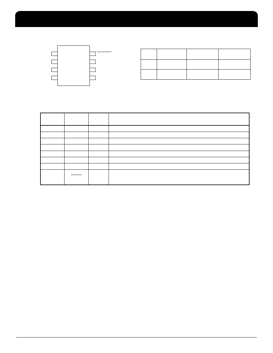
Pin Assignment
8-pin (150 mil) SOIC
Output Clock Selection Table
Pin Descriptions
External Components
The ICS252 requires a minimum number of external
components for proper operation.
Series Termination Resistor
Clock output traces over one inch should use series
termination. To series terminate a 50
trace (a commonly
used trace impedance), place a 33
resistor in series with
the clock line, as close to the clock output pin as possible.
The nominal impedance of the clock output is 20
.
Decoupling Capacitor
As with any high-performance mixed-signal IC, the ICS252
must be isolated from system power supply noise to perform
optimally.
A decoupling capacitor of 0.01F must be connected
between VDD and the PCB ground plane.
Crystal Load Capacitors
The device crystal connections should include pads for
small capacitors from X1 to ground and from X2 to ground.
These capacitors are used to adjust the stray capacitance
of the board to match the nominally required crystal load
capacitance. Because load capacitance can only be
increased in this trimming process, it is important to keep
stray capacitance to a minimum by using very short PCB
traces (and no vias) been the crystal and device. Crystal
capacitors must be connected from each of the pins X1 and
X2 to ground.
The value (in pF) of these crystal caps should equal (CL -6
pF)*2. In this equation, CL= crystal load capacitance in pF.
Example: For a crystal with a 16 pF load capacitance, each
crystal capacitor would be 20 pF [(16-6) x 2 = 20].
PCB Layout Recommendations
For optimum device performance and lowest output phase
X 1 /IC L K
VD D
G N D
SEL
CL K 2
CL K 1
X2
1
2
3
4
8
7
6
5
PD T S
SEL
CLK1 (MHz)
CLK2 (MHz)
Spread
Percentage
0
User
Configurable
User
Configurable
User
Configurable
1User
Configurable
User
Configurable
User
Configurable
Pin
Number
Pin
Name
Pin
Type
Pin Description
1
SEL
Input
Select pin for frequency selection on CLK1 and CLK2. Internal pull-up resistor.
2
VDD
Power
Connect to +3.3 V.
3
X1/ICLK
XI
Connect this pin to a crystal or external clock input.
4
X2
XO
Connect this pin to a crystal, or float for clock input.
5
CLK1
Output
Clock1 output. Weak internal pull-down, low when power down.
6
CLK2
Output
Clock2 output. Weak internal pull-down, low when power down.
7
GND
Power
Connect this to ground.
8PDTS
Input
Powers down entire chip. Tri-states CLK outputs when low. No internal pull-up
resistor. The pin must be tied either directly or through the external resistor to
VDD ro GND. External resistor value must be less than 15kOhm.
相关PDF资料 |
PDF描述 |
|---|---|
| ICS252PMT | 200 MHz, OTHER CLOCK GENERATOR, PDSO8 |
| ICS271GI-XXLF | 200 MHz, OTHER CLOCK GENERATOR, PDSO20 |
| ICS271GI-XXT | 200 MHz, OTHER CLOCK GENERATOR, PDSO20 |
| ICS271PGLF | 200 MHz, OTHER CLOCK GENERATOR, PDSO20 |
| ICS307G-03LF | 270 MHz, OTHER CLOCK GENERATOR, PDSO16 |
相关代理商/技术参数 |
参数描述 |
|---|---|
| ICS252PMILF | 功能描述:IC CLK SYNTHESIZER FP DUAL 8SOIC RoHS:是 类别:集成电路 (IC) >> 时钟/计时 - 时钟发生器,PLL,频率合成器 系列:VersaClock™ 标准包装:1,000 系列:Precision Edge® 类型:时钟/频率合成器 PLL:无 输入:CML,PECL 输出:CML 电路数:1 比率 - 输入:输出:2:1 差分 - 输入:输出:是/是 频率 - 最大:10.7GHz 除法器/乘法器:无/无 电源电压:2.375 V ~ 3.6 V 工作温度:-40°C ~ 85°C 安装类型:表面贴装 封装/外壳:16-VFQFN 裸露焊盘,16-MLF? 供应商设备封装:16-MLF?(3x3) 包装:带卷 (TR) 其它名称:SY58052UMGTRSY58052UMGTR-ND |
| ICS252PMILFT | 功能描述:IC CLK SYNTHESIZER FP DUAL 8SOIC RoHS:是 类别:集成电路 (IC) >> 时钟/计时 - 时钟发生器,PLL,频率合成器 系列:VersaClock™ 标准包装:2,000 系列:- 类型:PLL 时钟发生器 PLL:带旁路 输入:LVCMOS,LVPECL 输出:LVCMOS 电路数:1 比率 - 输入:输出:2:11 差分 - 输入:输出:是/无 频率 - 最大:240MHz 除法器/乘法器:是/无 电源电压:3.135 V ~ 3.465 V 工作温度:0°C ~ 70°C 安装类型:表面贴装 封装/外壳:32-LQFP 供应商设备封装:32-TQFP(7x7) 包装:带卷 (TR) |
| ICS252PMLF | 功能描述:IC CLK SYNTHESIZER FP DUAL 8SOIC RoHS:是 类别:集成电路 (IC) >> 时钟/计时 - 时钟发生器,PLL,频率合成器 系列:VersaClock™ 标准包装:2,000 系列:- 类型:PLL 时钟发生器 PLL:带旁路 输入:LVCMOS,LVPECL 输出:LVCMOS 电路数:1 比率 - 输入:输出:2:11 差分 - 输入:输出:是/无 频率 - 最大:240MHz 除法器/乘法器:是/无 电源电压:3.135 V ~ 3.465 V 工作温度:0°C ~ 70°C 安装类型:表面贴装 封装/外壳:32-LQFP 供应商设备封装:32-TQFP(7x7) 包装:带卷 (TR) |
| ICS252PMLFT | 功能描述:IC CLK SYNTHESIZER FP DUAL 8SOIC RoHS:是 类别:集成电路 (IC) >> 时钟/计时 - 时钟发生器,PLL,频率合成器 系列:VersaClock™ 标准包装:2,000 系列:- 类型:PLL 时钟发生器 PLL:带旁路 输入:LVCMOS,LVPECL 输出:LVCMOS 电路数:1 比率 - 输入:输出:2:11 差分 - 输入:输出:是/无 频率 - 最大:240MHz 除法器/乘法器:是/无 电源电压:3.135 V ~ 3.465 V 工作温度:0°C ~ 70°C 安装类型:表面贴装 封装/外壳:32-LQFP 供应商设备封装:32-TQFP(7x7) 包装:带卷 (TR) |
| ICS252PMT | 功能描述:IC CLK SYNTHESIZER FP DUAL 8SOIC RoHS:否 类别:集成电路 (IC) >> 时钟/计时 - 时钟发生器,PLL,频率合成器 系列:VersaClock™ 产品变化通告:Product Discontinuation 04/May/2011 标准包装:96 系列:- 类型:时钟倍频器,零延迟缓冲器 PLL:带旁路 输入:LVTTL 输出:LVTTL 电路数:1 比率 - 输入:输出:1:8 差分 - 输入:输出:无/无 频率 - 最大:133.3MHz 除法器/乘法器:是/无 电源电压:3 V ~ 3.6 V 工作温度:0°C ~ 70°C 安装类型:表面贴装 封装/外壳:16-TSSOP(0.173",4.40mm 宽) 供应商设备封装:16-TSSOP 包装:管件 其它名称:23S08-5HPGG |
发布紧急采购,3分钟左右您将得到回复。