- 您现在的位置:买卖IC网 > PDF目录65530 > ICS552R-01I LOW SKEW CLOCK DRIVER, PDSO20 PDF资料下载
参数资料
| 型号: | ICS552R-01I |
| 元件分类: | 时钟及定时 |
| 英文描述: | LOW SKEW CLOCK DRIVER, PDSO20 |
| 封装: | 0.150 INCH, SSOP-20 |
| 文件页数: | 7/10页 |
| 文件大小: | 184K |
| 代理商: | ICS552R-01I |
Oscillator, Multiplier, and Buffer with 8 Outputs
MDS 552-01 E
6
Revision 111705
Integrated Circuit Systems, Inc.
● 525 Race Street, San Jose, CA 95126 ● tel (408) 297-1201 ● www.icst.com
ICS552-01
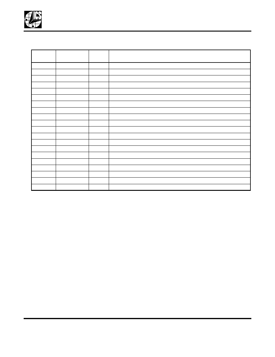
Pin Descriptions (ICS552-01—C mode)
External Components
Series Termination Resistor
Clock output traces over one inch should use series
termination. To series terminate a 50
trace (a
commonly used trace impedance), place a 33
resistor
in series with the clock line, as close to the clock output
pin as possible. The nominal impedance of the clock
output is 20
.
Decoupling Capacitors
As with any high-performance mixed-signal IC, the
ICS552-01 must be isolated from system power supply
noise to perform optimally.
Decoupling capacitors of 0.01F must be connected
between each VDD and GND on pins 4 and 6, and 16
and 14. Other VDDs and GNDs can be connected to
these pins or directly to their respective ground planes.
Crystal Load Capacitors
The device crystal connections should include pads for
small capacitors from X1 to ground and from X2 to
ground. These capacitors are used to adjust the stray
capacitance of the board to match the nominally
required crystal load capacitance. Because load
capacitance can only be increased in this trimming
process, it is important to keep stray capacitance to a
minimum by using very short PCB traces (and no vias)
been the crystal and device. Crystal capacitors must be
connected from each of the pins X1 and X2 to ground.
The value (in pF) of these crystal caps should equal
(CL -12 pF)*2. In this equation, CL= crystal load
capacitance in pF. Example: For a crystal with a 18 pF
load capacitance, two 12 pF capacitors should be
used. For a clock input, connect it X1/ICLK and leave
X2 unconnected (floating).
Pin
Number
Pin
Name
Pin
Type
Pin Description
1
DC
—
Do not connect.
2
X2
XO
Crystal connection. Connect to a 10 - 27 MHz fundamental mode crystal.
3
X1
XI
Crystal connection. Connect to a 10 - 27 MHz fundamental mode crystal.
4
VDD
Power
Connect to +3.3 V or 5 V. Decouple with pin 6. Must be same as other VDDs.
5GND
Power
Connect to ground.
6
GND
Power
Connect to ground.
7
CLK1
Output
Output clock 1.
8
CLK2
Output
Output clock 2.
9
CLK3
Output
Output clock 3.
10
CLK4
Output
Output clock 4.
11
VDD
Power
Connect to +3.3 V or 5 V. Must be same as other VDDs.
12
CLK5
Output
Output clock 5.
13
CLK6
Output
Output clock 6.
14
GND
Power
Connect to ground.
15
VDD
Power
Connect to +3.3 V or 5 V. Must be same as other VDDs.
16
VDD
Power
Connect to +3.3 V or 5 V. Decouple with pin 14. Must be same as other VDDs.
17
CLK7
Output
Output clock 7.
18
CLK8
Output
Output clock 8.
19
DC
—
Do not connect.
20
VDD
Power
Connect to +3.3 V or 5 V. Must be same as other VDDs.
相关PDF资料 |
PDF描述 |
|---|---|
| ICS552R-01IT | LOW SKEW CLOCK DRIVER, PDSO20 |
| ICS554G-01AI | 554 SERIES, LOW SKEW CLOCK DRIVER, 4 TRUE OUTPUT(S), 0 INVERTED OUTPUT(S), PDSO16 |
| ICS554G-01IT | LOW SKEW CLOCK DRIVER, 4 TRUE OUTPUT(S), 0 INVERTED OUTPUT(S), PDSO16 |
| ICS557G-06LFT | 557 SERIES, LOW SKEW CLOCK DRIVER, 4 TRUE OUTPUT(S), 0 INVERTED OUTPUT(S), PDSO20 |
| ICS557G-06T | 557 SERIES, LOW SKEW CLOCK DRIVER, 4 TRUE OUTPUT(S), 0 INVERTED OUTPUT(S), PDSO20 |
相关代理商/技术参数 |
参数描述 |
|---|---|
| ICS552R-01ILF | 功能描述:IC OSC/MULT/BUFFER OCT 20-SSOP RoHS:是 类别:集成电路 (IC) >> 时钟/计时 - 时钟发生器,PLL,频率合成器 系列:- 标准包装:2,000 系列:- 类型:PLL 时钟发生器 PLL:带旁路 输入:LVCMOS,LVPECL 输出:LVCMOS 电路数:1 比率 - 输入:输出:2:11 差分 - 输入:输出:是/无 频率 - 最大:240MHz 除法器/乘法器:是/无 电源电压:3.135 V ~ 3.465 V 工作温度:0°C ~ 70°C 安装类型:表面贴装 封装/外壳:32-LQFP 供应商设备封装:32-TQFP(7x7) 包装:带卷 (TR) |
| ICS552R-01ILFT | 功能描述:IC OSC/MULT/BUFFER OCT 20-SSOP RoHS:是 类别:集成电路 (IC) >> 时钟/计时 - 时钟发生器,PLL,频率合成器 系列:- 标准包装:2,000 系列:- 类型:PLL 时钟发生器 PLL:带旁路 输入:LVCMOS,LVPECL 输出:LVCMOS 电路数:1 比率 - 输入:输出:2:11 差分 - 输入:输出:是/无 频率 - 最大:240MHz 除法器/乘法器:是/无 电源电压:3.135 V ~ 3.465 V 工作温度:0°C ~ 70°C 安装类型:表面贴装 封装/外壳:32-LQFP 供应商设备封装:32-TQFP(7x7) 包装:带卷 (TR) |
| ICS552R-01IT | 功能描述:IC OSC/MULT/BUFFER OCT 20-SSOP RoHS:否 类别:集成电路 (IC) >> 时钟/计时 - 时钟发生器,PLL,频率合成器 系列:- 产品变化通告:Product Discontinuation 04/May/2011 标准包装:96 系列:- 类型:时钟倍频器,零延迟缓冲器 PLL:带旁路 输入:LVTTL 输出:LVTTL 电路数:1 比率 - 输入:输出:1:8 差分 - 输入:输出:无/无 频率 - 最大:133.3MHz 除法器/乘法器:是/无 电源电压:3 V ~ 3.6 V 工作温度:0°C ~ 70°C 安装类型:表面贴装 封装/外壳:16-TSSOP(0.173",4.40mm 宽) 供应商设备封装:16-TSSOP 包装:管件 其它名称:23S08-5HPGG |
| ICS552R-01LN | 功能描述:IC OSC/MULT/BUFFER OCT 20-SSOP RoHS:是 类别:集成电路 (IC) >> 时钟/计时 - 时钟发生器,PLL,频率合成器 系列:- 标准包装:2,000 系列:- 类型:PLL 时钟发生器 PLL:带旁路 输入:LVCMOS,LVPECL 输出:LVCMOS 电路数:1 比率 - 输入:输出:2:11 差分 - 输入:输出:是/无 频率 - 最大:240MHz 除法器/乘法器:是/无 电源电压:3.135 V ~ 3.465 V 工作温度:0°C ~ 70°C 安装类型:表面贴装 封装/外壳:32-LQFP 供应商设备封装:32-TQFP(7x7) 包装:带卷 (TR) |
| ICS552R-01LNT | 功能描述:IC OSC/MULT/BUFFER OCT 20-SSOP RoHS:是 类别:集成电路 (IC) >> 时钟/计时 - 时钟发生器,PLL,频率合成器 系列:- 标准包装:2,000 系列:- 类型:PLL 时钟发生器 PLL:带旁路 输入:LVCMOS,LVPECL 输出:LVCMOS 电路数:1 比率 - 输入:输出:2:11 差分 - 输入:输出:是/无 频率 - 最大:240MHz 除法器/乘法器:是/无 电源电压:3.135 V ~ 3.465 V 工作温度:0°C ~ 70°C 安装类型:表面贴装 封装/外壳:32-LQFP 供应商设备封装:32-TQFP(7x7) 包装:带卷 (TR) |
发布紧急采购,3分钟左右您将得到回复。