- 您现在的位置:买卖IC网 > PDF目录1997 > ICS843001AG-21LFT (IDT, Integrated Device Technology Inc)IC SYNTHESIZER LVPECL 24-TSSOP PDF资料下载
参数资料
| 型号: | ICS843001AG-21LFT |
| 厂商: | IDT, Integrated Device Technology Inc |
| 文件页数: | 3/17页 |
| 文件大小: | 0K |
| 描述: | IC SYNTHESIZER LVPECL 24-TSSOP |
| 标准包装: | 2,500 |
| 系列: | HiPerClockS™, FemtoClock™ |
| 类型: | 频率合成器 |
| PLL: | 带旁路 |
| 输入: | 晶体 |
| 输出: | LVCMOS,LVPECL,LVTTL |
| 电路数: | 1 |
| 比率 - 输入:输出: | 2:2 |
| 差分 - 输入:输出: | 无/是 |
| 频率 - 最大: | 700MHz |
| 除法器/乘法器: | 是/无 |
| 电源电压: | 3.135 V ~ 3.465 V |
| 工作温度: | 0°C ~ 70°C |
| 安装类型: | 表面贴装 |
| 封装/外壳: | 24-TSSOP(0.173",4.40mm 宽) |
| 供应商设备封装: | 24-TSSOP |
| 包装: | 带卷 (TR) |
| 其它名称: | 843001AG-21LFT |
ICS843001-21
FEMTOCLOCKS CRYSTAL-TO-3.3V LVPECL FREQUENCY SYNTHESIZER
IDT / ICS LVPECL FREQUENCY SYNTHESIZER
11
ICS843001AG-21 REV. AMARCH 15, 2007
Recommendations for Unused Input and Output Pins
Inputs:
Crystal Inputs:
For applications not requiring the use of the crystal oscillator input,
both XTAL_IN and XTAL_OUT can be left floating. Though not
required, but for additional protection, a 1k
resistor can be tied
from XTAL_IN to ground.
TEST_CLK Input:
For applications not requiring the use of the test clock, it can be left
floating. Though not required, but for additional protection, a 1k
resistor can be tied from the TEST_CLK to ground.
LVCMOS Control Pins:
All control pins have internal pull-ups or pull-downs; additional
resistance is not required but can be added for additional
protection. A 1k
resistor can be used.
Outputs:
LVPECL Output:
All unused LVPECL outputs can be left floating. We recommend
that there is no trace attached. Both sides of the differential output
pair should either be left floating or terminated.
LVCMOS Output:
All unused LVCMOS output can be left floating. We recommend
that there is no trace attached.
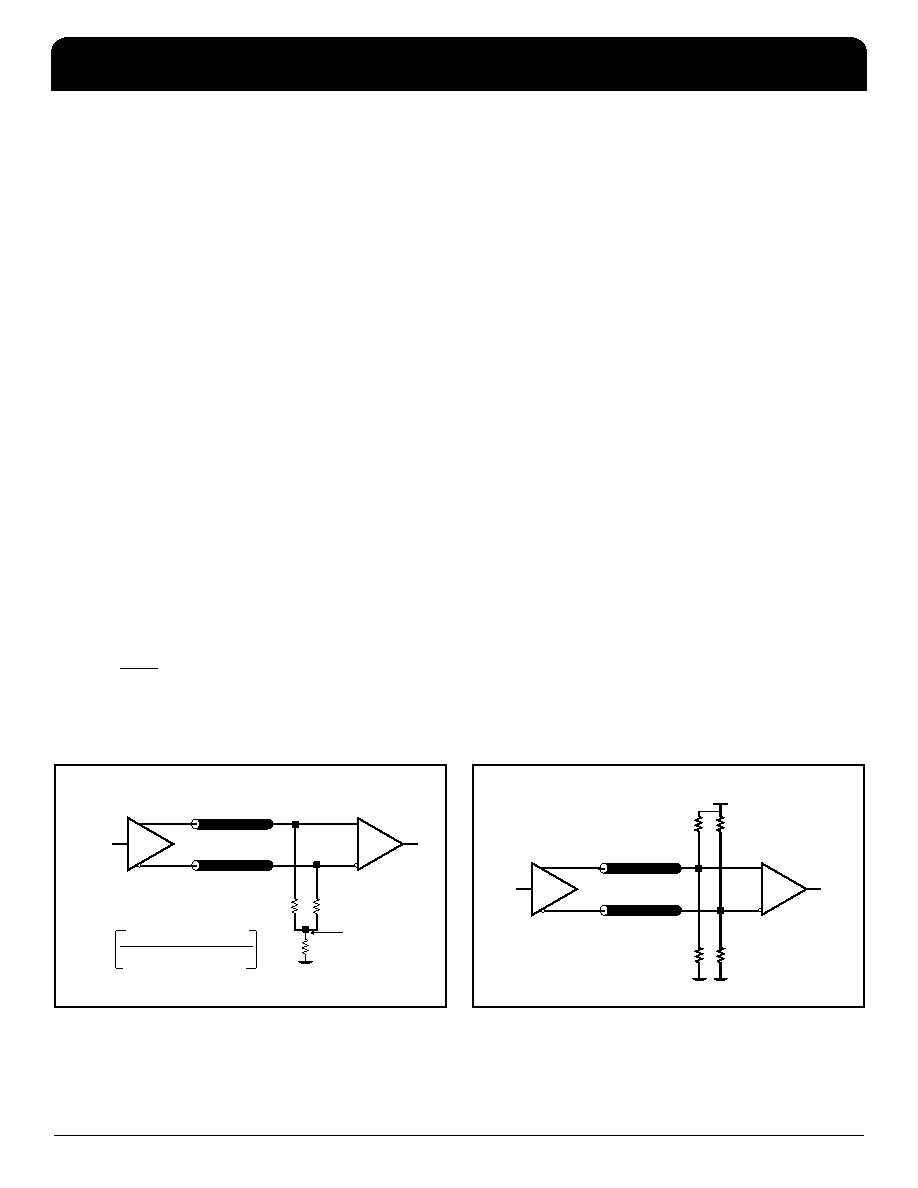
Termination for 3.3V LVPECL Outputs
The clock layout topology shown below is a typical termination for
LVPECL outputs. The two different layouts mentioned are
recommended only as guidelines.
FOUT and FOUT are low impedance follower outputs that
generate ECL/LVPECL compatible outputs. Therefore, terminating
resistors (DC current path to ground) or current sources must be
used for functionality. These outputs are designed to drive 50
transmission lines. Matched impedance techniques should be
used to maximize operating frequency and minimize signal
distortion. Figures 4A and 4B show two different layouts which are
recommended only as guidelines. Other suitable clock layouts may
exist and it would be recommended that the board designers
simulate to guarantee compatibility across all printed circuit and
clock component process variations.
Figure 4A. 3.3V LVPECL Output Termination
Figure 4B. 3.3V LVPECL Output Termination
V
CC - 2V
50
50
RTT
Z
o = 50
Z
o = 50
FOUT
FIN
RTT =
Z
o
1
((V
OH + VOL) / (VCC – 2)) – 2
3.3V
125
125
84
84
Z
o = 50
Z
o = 50
FOUT
FIN
相关PDF资料 |
PDF描述 |
|---|---|
| ICS843001AGI-22LFT | IC SYNTHESIZER LVPECL 24-TSSOP |
| ICS843001AKI-40LF | IC SYNTHESIZER LVPECL 16-VFQFPN |
| ICS843002AGI-01LF | IC SYNTHESIZER LVPECL 20-TSSOP |
| ICS843002AKI-41LF | IC SYNTHESIZER LVPECL 32-VFQFPN |
| ICS843004AG-02LF | IC SYNTHESIZER LVPECL 24-TSSOP |
相关代理商/技术参数 |
参数描述 |
|---|---|
| ICS843001AG-21T | 制造商:ICS 制造商全称:ICS 功能描述:FEMTOCLOCKS⑩ CRYSTAL-TO-3.3V LVPECL FREQUENCY SYNTHESIZER |
| ICS843001AGI-22 | 制造商:ICS 制造商全称:ICS 功能描述:FEMTOCLOCKS? CRYSTAL/LVCMOS-TO-3.3V, 2.5V LVPECL FREQUENCY SYNTHESIZER |
| ICS843001AGI-22LF | 功能描述:IC SYNTHESIZER LVPECL 24-TSSOP RoHS:是 类别:集成电路 (IC) >> 时钟/计时 - 时钟发生器,PLL,频率合成器 系列:HiPerClockS™, FemtoClock™ 标准包装:1,000 系列:Precision Edge® 类型:时钟/频率合成器 PLL:无 输入:CML,PECL 输出:CML 电路数:1 比率 - 输入:输出:2:1 差分 - 输入:输出:是/是 频率 - 最大:10.7GHz 除法器/乘法器:无/无 电源电压:2.375 V ~ 3.6 V 工作温度:-40°C ~ 85°C 安装类型:表面贴装 封装/外壳:16-VFQFN 裸露焊盘,16-MLF? 供应商设备封装:16-MLF?(3x3) 包装:带卷 (TR) 其它名称:SY58052UMGTRSY58052UMGTR-ND |
| ICS843001AGI-22LFT | 功能描述:IC SYNTHESIZER LVPECL 24-TSSOP RoHS:是 类别:集成电路 (IC) >> 时钟/计时 - 时钟发生器,PLL,频率合成器 系列:HiPerClockS™, FemtoClock™ 标准包装:27 系列:Precision Edge® 类型:频率合成器 PLL:是 输入:PECL,晶体 输出:PECL 电路数:1 比率 - 输入:输出:1:1 差分 - 输入:输出:无/是 频率 - 最大:800MHz 除法器/乘法器:是/无 电源电压:3.135 V ~ 5.25 V 工作温度:0°C ~ 85°C 安装类型:表面贴装 封装/外壳:28-SOIC(0.295",7.50mm 宽) 供应商设备封装:28-SOIC 包装:管件 |
| ICS843001AGI-22T | 制造商:ICS 制造商全称:ICS 功能描述:FEMTOCLOCKS? CRYSTAL/LVCMOS-TO-3.3V, 2.5V LVPECL FREQUENCY SYNTHESIZER |
发布紧急采购,3分钟左右您将得到回复。