- 您现在的位置:买卖IC网 > PDF目录9578 > ICS8430S10BYI-02LFT (IDT, Integrated Device Technology Inc)IC CLK GENERATOR PLL 48TQFP PDF资料下载
参数资料
| 型号: | ICS8430S10BYI-02LFT |
| 厂商: | IDT, Integrated Device Technology Inc |
| 文件页数: | 11/31页 |
| 文件大小: | 0K |
| 描述: | IC CLK GENERATOR PLL 48TQFP |
| 标准包装: | 1,000 |
| 类型: | 时钟/频率发生器,扇出缓冲器(分配),多路复用器 |
| PLL: | 是 |
| 主要目的: | Cavium 处理器 |
| 输入: | LVCMOS,LVDS,LVPECL,LVTTL,SSTL,晶体 |
| 输出: | LVCMOS,LVDS,LVPECL,LVTTL |
| 电路数: | 1 |
| 比率 - 输入:输出: | 2:10 |
| 差分 - 输入:输出: | 是/是 |
| 频率 - 最大: | 133.33MHz |
| 电源电压: | 3.135 V ~ 3.465 V |
| 工作温度: | -40°C ~ 85°C |
| 安装类型: | 表面贴装 |
| 封装/外壳: | 48-TQFP 裸露焊盘 |
| 供应商设备封装: | 48-PTQFP-EP(7x7) |
| 包装: | 带卷 (TR) |
第1页第2页第3页第4页第5页第6页第7页第8页第9页第10页当前第11页第12页第13页第14页第15页第16页第17页第18页第19页第20页第21页第22页第23页第24页第25页第26页第27页第28页第29页第30页第31页
ICS8430S10BYI-02 REVISION C JANUARY 17, 2011
19
2011 Integrated Device Technology, Inc.
ICS8430S10I-02 Data Sheet
CLOCK GENERATOR FOR CAVIUM PROCESSORS
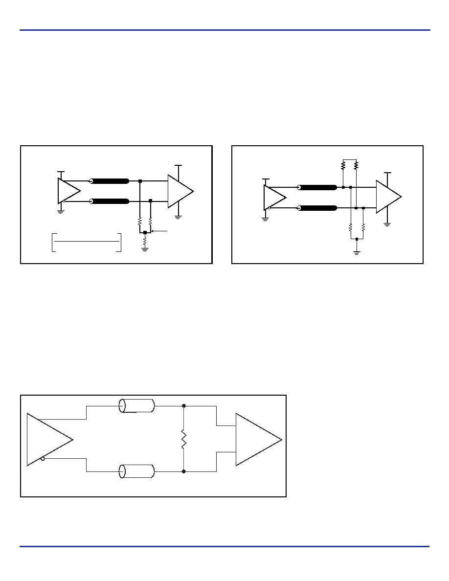
Termination for 3.3V LVPECL Outputs
The clock layout topology shown below is a typical termination for
LVPECL outputs. The two different layouts mentioned are
recommended only as guidelines.
The differential output pair is low impedance follower outputs that
generate ECL/LVPECL compatible outputs. Therefore, terminating
resistors (DC current path to ground) or current sources must be
used for functionality. These outputs are designed to drive 50
transmission lines. Matched impedance techniques should be used
to maximize operating frequency and minimize signal distortion.
Figures 4A and 4B show two different layouts which are
recommended only as guidelines. Other suitable clock layouts may
exist and it would be recommended that the board designers
simulate to guarantee compatibility across all printed circuit and clock
component process variations.
Figure 4A. 3.3V LVPECL Output Termination
Figure 4B. 3.3V LVPECL Output Termination
LVDS Driver Termination
A general LVDS interface is shown in Figure 5. Standard termination
for LVDS type output structure requires both a 100
parallel resistor
at the receiver and a 100
differential transmission line environment.
In order to avoid any transmission line reflection issues, the 100
resistor must be placed as close to the receiver as possible. IDT
offers a full line of LVDS compliant devices with two types of output
structures: current source and voltage source. The standard
termination schematic as shown in Figure 5 can be used with either
type of output structure. If using a non-standard termination, it is
recommended to contact IDT and confirm if the output is a current
source or a voltage source type structure. In addition, since these
outputs are LVDS compatible, the amplitude and common mode
input range of the input receivers should be verified for compatibility
with the output.
Figure 5. Typical LVDS Driver Termination
3.3V
V
CC - 2V
R1
50
R2
50
RTT
Z
o = 50
Z
o = 50
+
_
RTT =
* Z
o
1
((V
OH + VOL) / (VCC – 2)) – 2
3.3V
LVPECL
Input
R1
84
R2
84
3.3V
R3
125
R4
125
Z
o = 50
Z
o = 50
LVPECL
Input
3.3V
+
_
100
–
+
100
Differential Transmission Line
LVDS Driver
LVDS
Receiver
相关PDF资料 |
PDF描述 |
|---|---|
| VI-B1L-IU | CONVERTER MOD DC/DC 28V 200W |
| VI-B1D-IU | CONVERTER MOD DC/DC 85V 200W |
| VE-2N4-MX-F4 | CONVERTER MOD DC/DC 48V 75W |
| MS3106A28-12S | CONN PLUG 26POS STRAIGHT W/SCKT |
| MS3451W14S-5P | CONN RCPT 5POS CBL MNT W/PINS |
相关代理商/技术参数 |
参数描述 |
|---|---|
| ICS8430S10I-03 | 制造商:IDT 制造商全称:Integrated Device Technology 功能描述:Clock Generator for Cavium Processors |
| ICS8431-01 | 制造商:ICS 制造商全称:ICS 功能描述:200MHZ, LOW JITTER, LVPECL FREQUENCY SYNTHESIZER |
| ICS843101-312 | 制造商:ICS 制造商全称:ICS 功能描述:FEMTOCLOCKS⑩ CRYSTAL-TO-LVPECL 312.5MHZ FREQUENCY MARGINING SYNTHESIZER |
| ICS843101AG-312 | 制造商:ICS 制造商全称:ICS 功能描述:FEMTOCLOCKS⑩ CRYSTAL-TO-LVPECL 312.5MHZ FREQUENCY MARGINING SYNTHESIZER |
| ICS843101AG-312LF | 制造商:ICS 制造商全称:ICS 功能描述:FEMTOCLOCKS⑩ CRYSTAL-TO-LVPECL 312.5MHZ FREQUENCY MARGINING SYNTHESIZER |
发布紧急采购,3分钟左右您将得到回复。