- 您现在的位置:买卖IC网 > PDF目录9578 > ICS8430S10BYI-02LFT (IDT, Integrated Device Technology Inc)IC CLK GENERATOR PLL 48TQFP PDF资料下载
参数资料
| 型号: | ICS8430S10BYI-02LFT |
| 厂商: | IDT, Integrated Device Technology Inc |
| 文件页数: | 13/31页 |
| 文件大小: | 0K |
| 描述: | IC CLK GENERATOR PLL 48TQFP |
| 标准包装: | 1,000 |
| 类型: | 时钟/频率发生器,扇出缓冲器(分配),多路复用器 |
| PLL: | 是 |
| 主要目的: | Cavium 处理器 |
| 输入: | LVCMOS,LVDS,LVPECL,LVTTL,SSTL,晶体 |
| 输出: | LVCMOS,LVDS,LVPECL,LVTTL |
| 电路数: | 1 |
| 比率 - 输入:输出: | 2:10 |
| 差分 - 输入:输出: | 是/是 |
| 频率 - 最大: | 133.33MHz |
| 电源电压: | 3.135 V ~ 3.465 V |
| 工作温度: | -40°C ~ 85°C |
| 安装类型: | 表面贴装 |
| 封装/外壳: | 48-TQFP 裸露焊盘 |
| 供应商设备封装: | 48-PTQFP-EP(7x7) |
| 包装: | 带卷 (TR) |
第1页第2页第3页第4页第5页第6页第7页第8页第9页第10页第11页第12页当前第13页第14页第15页第16页第17页第18页第19页第20页第21页第22页第23页第24页第25页第26页第27页第28页第29页第30页第31页
ICS8430S10BYI-02 REVISION C JANUARY 17, 2011
20
2011 Integrated Device Technology, Inc.
ICS8430S10I-02 Data Sheet
CLOCK GENERATOR FOR CAVIUM PROCESSORS
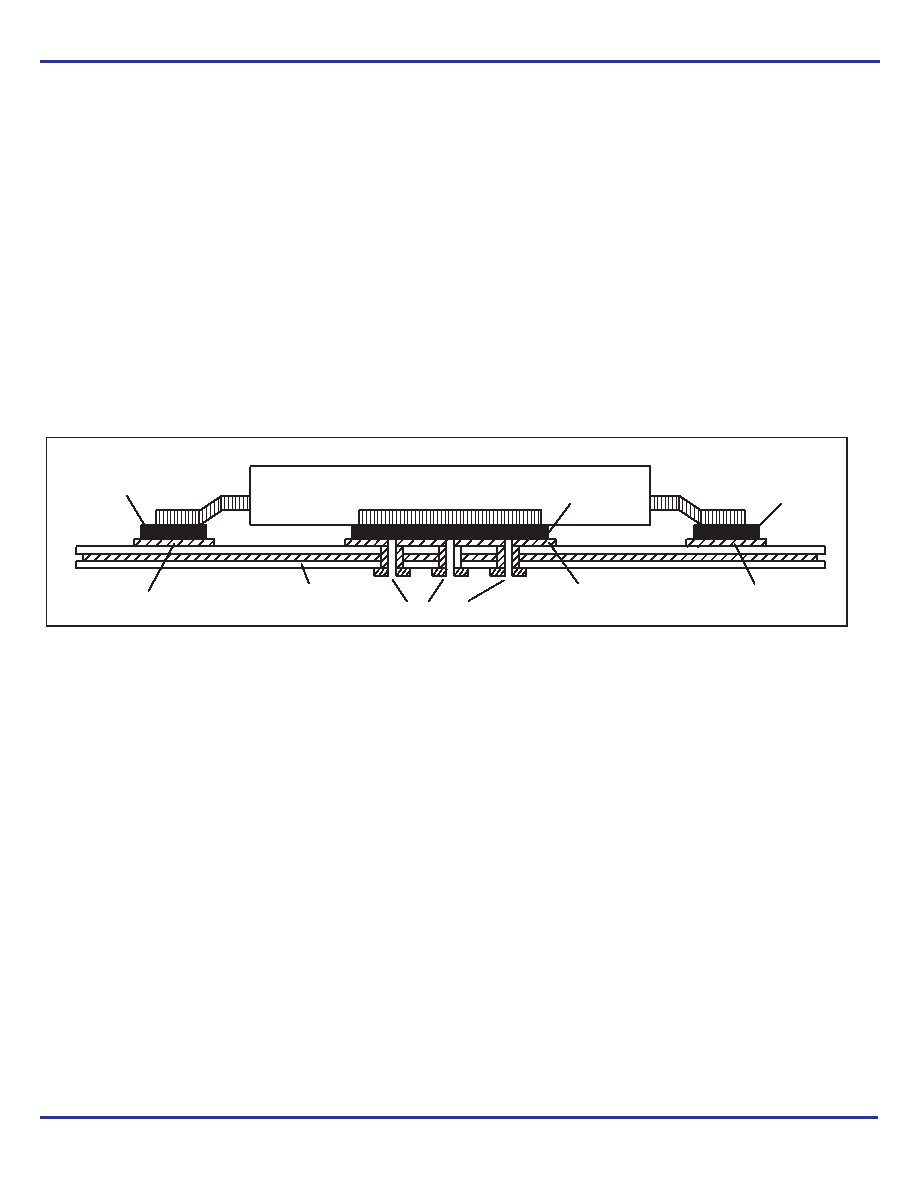
EPAD Thermal Release Path
In order to maximize both the removal of heat from the package and
the electrical performance, a land pattern must be incorporated on
the Printed Circuit Board (PCB) within the footprint of the package
corresponding to the exposed metal pad or exposed heat slug on the
package, as shown in Figure 6. The solderable area on the PCB, as
defined by the solder mask, should be at least the same size/shape
as the exposed pad/slug area on the package to maximize the
thermal/electrical performance. Sufficient clearance should be
designed on the PCB between the outer edges of the land pattern
and the inner edges of pad pattern for the leads to avoid any shorts.
While the land pattern on the PCB provides a means of heat transfer
and electrical grounding from the package to the board through a
solder joint, thermal vias are necessary to effectively conduct from
the surface of the PCB to the ground plane(s). The land pattern must
be connected to ground through these vias. The vias act as “heat
pipes”. The number of vias (i.e. “heat pipes”) are application specific
and dependent upon the package power dissipation as well as
electrical conductivity requirements. Thus, thermal and electrical
analysis and/or testing are recommended to determine the minimum
number needed. Maximum thermal and electrical performance is
achieved when an array of vias is incorporated in the land pattern. It
is recommended to use as many vias connected to ground as
possible. It is also recommended that the via diameter should be 12
to 13mils (0.30 to 0.33mm) with 1oz copper via barrel plating. This is
desirable to avoid any solder wicking inside the via during the
soldering process which may result in voids in solder between the
exposed pad/slug and the thermal land. Precautions should be taken
to eliminate any solder voids between the exposed heat slug and the
land pattern. Note: These recommendations are to be used as a
guideline only. For further information, please refer to the Application
Note on the Surface Mount Assembly of Amkor’s Thermally/
Electrically Enhance Leadframe Base Package, Amkor Technology.
Figure 6. P.C. Assembly for Exposed Pad Thermal Release Path – Side View (drawing not to scale)
Recommendations for Unused Input and Output Pins
Inputs:
CLK/nCLK Inputs
For applications not requiring the use of the differential input, both
CLK and nCLK can be left floating. Though not required, but for
additional protection, a 1k
resistor can be tied from CLK to ground.
Crystal Inputs
For applications not requiring the use of the crystal oscillator input,
both XTAL_IN and XTAL_OUT can be left floating. Though not
required, but for additional protection, a 1k
resistor can be tied from
XTAL_IN to ground.
LVCMOS Control Pins
All control pins have internal pulldowns; additional resistance is not
required but can be added for additional protection. A 1k
resistor
can be used.
Outputs:
LVPECL Outputs
All unused LVPECL outputs can be left floating. We recommend that
there is no trace attached. Both sides of the differential output pair
should either be left floating or terminated.
LVDS Outputs
All unused LVDS output pairs can be either left floating or terminated
with 100
across. If they are left floating, there should be no trace
attached.
LVCMOS Outputs
All unused LVCMOS output can be left floating. There should be no
trace attached.
GROUND PLANE
LAND PATTERN
SOLDER
THERMAL VIA
EXPOSED HEAT SLUG
(GROUND PAD)
PIN
PIN PAD
SOLDER
PIN
PIN PAD
SOLDER
相关PDF资料 |
PDF描述 |
|---|---|
| VI-B1L-IU | CONVERTER MOD DC/DC 28V 200W |
| VI-B1D-IU | CONVERTER MOD DC/DC 85V 200W |
| VE-2N4-MX-F4 | CONVERTER MOD DC/DC 48V 75W |
| MS3106A28-12S | CONN PLUG 26POS STRAIGHT W/SCKT |
| MS3451W14S-5P | CONN RCPT 5POS CBL MNT W/PINS |
相关代理商/技术参数 |
参数描述 |
|---|---|
| ICS8430S10I-03 | 制造商:IDT 制造商全称:Integrated Device Technology 功能描述:Clock Generator for Cavium Processors |
| ICS8431-01 | 制造商:ICS 制造商全称:ICS 功能描述:200MHZ, LOW JITTER, LVPECL FREQUENCY SYNTHESIZER |
| ICS843101-312 | 制造商:ICS 制造商全称:ICS 功能描述:FEMTOCLOCKS⑩ CRYSTAL-TO-LVPECL 312.5MHZ FREQUENCY MARGINING SYNTHESIZER |
| ICS843101AG-312 | 制造商:ICS 制造商全称:ICS 功能描述:FEMTOCLOCKS⑩ CRYSTAL-TO-LVPECL 312.5MHZ FREQUENCY MARGINING SYNTHESIZER |
| ICS843101AG-312LF | 制造商:ICS 制造商全称:ICS 功能描述:FEMTOCLOCKS⑩ CRYSTAL-TO-LVPECL 312.5MHZ FREQUENCY MARGINING SYNTHESIZER |
发布紧急采购,3分钟左右您将得到回复。