- 您现在的位置:买卖IC网 > PDF目录65533 > ICS9112CM-18LFT (INTEGRATED DEVICE TECHNOLOGY INC) PLL BASED CLOCK DRIVER, 8 TRUE OUTPUT(S), 0 INVERTED OUTPUT(S), PDSO16 PDF资料下载
参数资料
| 型号: | ICS9112CM-18LFT |
| 厂商: | INTEGRATED DEVICE TECHNOLOGY INC |
| 元件分类: | 时钟及定时 |
| 英文描述: | PLL BASED CLOCK DRIVER, 8 TRUE OUTPUT(S), 0 INVERTED OUTPUT(S), PDSO16 |
| 封装: | 0.150 INCH, SOIC-16 |
| 文件页数: | 3/5页 |
| 文件大小: | 84K |
| 代理商: | ICS9112CM-18LFT |
ZERO DELAY, LOW SKEW BUFFER
MDS 9112CM-18 B
3
Revision 021903
Int egrat ed C i rcuit Syste ms q 525 R a ce S t r eet, San Jose, CA 95126 q t e l (40 8 ) 295 -9800 q
w w w. icst . c om
ICS9112CM-18
External Components
The ICS9112CM-18 requires a minimum number of external components for proper operation. Decoupling
capacitors of 0.1
F should be connected between VDD and GND, as close to the part as possible. A 33
series terminating resistor should be used on each clock output to reduce reflections.
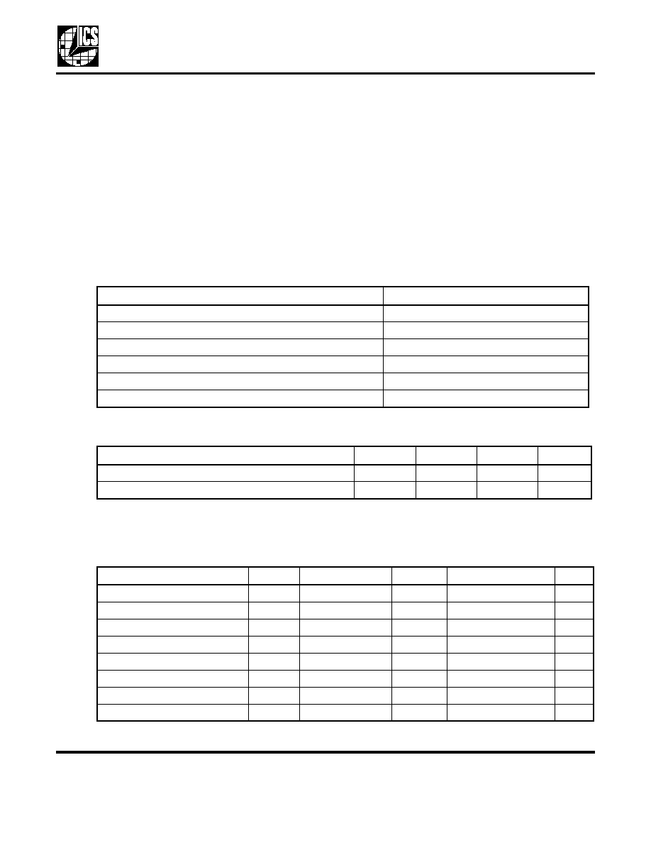
Absolute Maximum Ratings
Stresses above the ratings listed below can cause permanent damage to the ICS9112CM-18. These
ratings, which are standard values for ICS commercially rated parts, are stress ratings only. Functional
operation of the device at these or any other conditions above those indicated in the operational sections
of the specifications is not implied. Exposure to absolute maximum rating conditions for extended periods
can affect product reliability. Electrical parameters are guaranteed only over the recommended operating
temperature range.
Recommended Operation Conditions
DC Electrical Characteristics
VDD=3.3 V ±10%, Ambient temperature 0 to +70
°C
Item
Rating
Supply Voltage, VDD
7 V
All Inputs and Outputs
-0.5 V to VDD+0.5 V
Ambient Operating Temperature
0 to +70
°C
Storage Temperature
-65 to +150
°C
Junction Temperature
175
°C
Soldering Temperature
260
°C
Parameter
Min.
Typ.
Max.
Units
Ambient Operating Temperature
0
+70
°C
Power Supply Voltage (measured in respect to GND)
+3.0
+5.5
V
Parameter
Symbol
Conditions
Min.
Typ.
Max.
Units
Operating Voltage
VDD
3.0
5.5
V
Input High Voltage
VIH
CLKIN pin only
(VDD/2)+1
VDD/2
V
Input Low Voltage
VIL
CLKIN pin only
VDD/2
(VDD/2)-1
V
Input High Voltage
VIH
2V
Input Low Voltage
VIL
0.8
V
Output High Voltage
VOH
IOH = -18mA
2.4
V
Output Low Voltage
VOL
IOL = 18mA
0.4
V
Output High Voltage
VOH
IOH = -5mA
VDD-0.4
V
相关PDF资料 |
PDF描述 |
|---|---|
| ICS9112CM-18 | PLL BASED CLOCK DRIVER, 8 TRUE OUTPUT(S), 0 INVERTED OUTPUT(S), PDSO16 |
| ICS9112M-16LF | 91 SERIES, LOW SKEW CLOCK DRIVER, 5 TRUE OUTPUT(S), 0 INVERTED OUTPUT(S), PDSO8 |
| ICS9112M-16 | 91 SERIES, LOW SKEW CLOCK DRIVER, 5 TRUE OUTPUT(S), 0 INVERTED OUTPUT(S), PDSO8 |
| ICS9112M-16-T | LOW SKEW CLOCK DRIVER, 5 TRUE OUTPUT(S), 0 INVERTED OUTPUT(S), PDSO8 |
| ICS9112M-16LF | 91 SERIES, LOW SKEW CLOCK DRIVER, 5 TRUE OUTPUT(S), 0 INVERTED OUTPUT(S), PDSO8 |
相关代理商/技术参数 |
参数描述 |
|---|---|
| ICS9112M-06 | 制造商:Integrated Device Technology Inc 功能描述: |
| ICS9112M-07 | 制造商:ICS 制造商全称:ICS 功能描述:Low Skew Output Buffer |
| ICS9112M-22 | 功能描述:IC CLK BUFFER DVR 133MHZ 8-SOIC RoHS:否 类别:集成电路 (IC) >> 时钟/计时 - 时钟缓冲器,驱动器 系列:- 标准包装:74 系列:- 类型:扇出缓冲器(分配) 电路数:1 比率 - 输入:输出:1:10 差分 - 输入:输出:是/是 输入:HCSL, LVCMOS, LVDS, LVPECL, LVTTL 输出:HCSL,LVDS 频率 - 最大:400MHz 电源电压:3 V ~ 3.6 V 工作温度:-40°C ~ 85°C 安装类型:表面贴装 封装/外壳:32-VFQFN 裸露焊盘 供应商设备封装:32-QFN(5x5) 包装:管件 |
| ICS9112M-31 | 制造商:ICS 制造商全称:ICS 功能描述:Frequency Generator for Fibre Channel Systems |
| ICS9112M-32 | 制造商:ICS 制造商全称:ICS 功能描述:Frequency Generator for Fibre Channel Systems |
发布紧急采购,3分钟左右您将得到回复。