- 您现在的位置:买卖IC网 > PDF目录65534 > ICS9112YM-17-T PLL BASED CLOCK DRIVER, 8 TRUE OUTPUT(S), 0 INVERTED OUTPUT(S), PDSO16 PDF资料下载
参数资料
| 型号: | ICS9112YM-17-T |
| 元件分类: | 时钟及定时 |
| 英文描述: | PLL BASED CLOCK DRIVER, 8 TRUE OUTPUT(S), 0 INVERTED OUTPUT(S), PDSO16 |
| 封装: | 0.150 INCH, MS-012, SOIC-16 |
| 文件页数: | 1/8页 |
| 文件大小: | 108K |
| 代理商: | ICS9112YM-17-T |
Integrated
Circuit
Systems, Inc.
General Description
Features
ICS9112-17
0051J—02/05/04
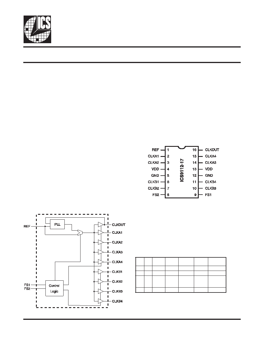
Block Diagram
Low Skew Output Buffer
Pin Configuration
Zero input - output delay
Frequency range 25 - 133 MHz (3.3V)
High loop filter bandwidth ideal for Spread Spectrum
applications.
Less than 200 ps cycle to cycle Jitter
Skew controlled outputs
Skew less than 250 ps between outputs
Available in 16 pin, 150 mil SSOP & SOIC package
The ICS9112-17 is a high performance, low skew, low jitter
zero delay buffer.
It uses a phase lock loop (PLL)
technology to align, in both phase and frequency, the REF
input with the CLKOUT signal. It is designed to distribute
high speed clocks in PC systems operating at speeds
from 25 to 133 MHz.
ICS9112-17 is a zero delay buffer that provides
synchronization between the input and output. The
synchronization is established via CLKOUT feed back to
the input of the PLL. Since the skew between the input and
output is less than +/- 350 pS, the part acts as a zero delay
buffer.
The ICS9112-17 has two banks of four outputs controlled
by two address lines. Depending on the selected address
line, bank B or both banks can be put in a tri-state mode.
In this mode, the PLL is still running and only the output
buffers are put in a high impedance mode. The test mode
shuts off the PLL and connects the input directly to the
output buffers (see table below for functionality).
The ICS9112-17 comes in a sixteen pin 150 mil SOIC or
16 pin SSOP package. In the absence of REF input, will
be in the power down mode. In this mode, the PLL is turned
off and the output buffers are pulled low. Power down mode
provides the lowest power consumption for a standby
condition.
2
S
F1
S
F
A
K
L
C
)
4
,
1
(
B
K
L
C
)
4
,
1
(
T
U
O
K
L
C
t
u
p
t
u
O
e
c
r
u
o
S
L
P
n
w
o
d
t
u
h
S
00
e
t
a
t
s
i
r
Te
t
a
t
s
i
r
Tn
e
v
i
r
DL
L
PN
01
n
e
v
i
r
De
t
a
t
s
i
r
Tn
e
v
i
r
DL
L
PN
10
L
P
s
a
p
y
B
e
d
o
M
L
P
s
a
p
y
B
e
d
o
M
L
P
s
a
p
y
B
e
d
o
M
F
E
RY
11
n
e
v
i
r
Dn
e
v
i
r
Dn
e
v
i
r
DL
L
PN
Functionality
16 pin SSOP & SOIC
相关PDF资料 |
PDF描述 |
|---|---|
| ICS9112YF-17-T | PLL BASED CLOCK DRIVER, 8 TRUE OUTPUT(S), 0 INVERTED OUTPUT(S), PDSO16 |
| ICS9112YM-26LF-T | LOW SKEW CLOCK DRIVER, 4 TRUE OUTPUT(S), 0 INVERTED OUTPUT(S), PDSO8 |
| ICS9112YM-26LFT | 9112 SERIES, LOW SKEW CLOCK DRIVER, 4 TRUE OUTPUT(S), 0 INVERTED OUTPUT(S), PDSO8 |
| ICS9112YM-28LF-T | 9112 SERIES, LOW SKEW CLOCK DRIVER, 5 TRUE OUTPUT(S), 0 INVERTED OUTPUT(S), PDSO8 |
| ICS9112YM-28LF-T | 9112 SERIES, LOW SKEW CLOCK DRIVER, 5 TRUE OUTPUT(S), 0 INVERTED OUTPUT(S), PDSO8 |
相关代理商/技术参数 |
参数描述 |
|---|---|
| ICS9112YM-27-T | 制造商:ICS 制造商全称:ICS 功能描述:Low Skew PCI / PCI-X Buffer |
| ICS9112YM-28LF-T | 制造商:ICS 制造商全称:ICS 功能描述:Low Skew Output Buffer |
| ICS9117-01 | 制造商:ICS 制造商全称:ICS 功能描述:Frequency Generator for Modem Systems |
| ICS9117M-01 | 制造商:ICS 制造商全称:ICS 功能描述:Frequency Generator for Modem Systems |
| ICS9117M02 | 制造商:未知厂家 制造商全称:未知厂家 功能描述:Peripheral IC |
发布紧急采购,3分钟左右您将得到回复。