- 您现在的位置:买卖IC网 > PDF目录65534 > ICS9112YM-17-T PLL BASED CLOCK DRIVER, 8 TRUE OUTPUT(S), 0 INVERTED OUTPUT(S), PDSO16 PDF资料下载
参数资料
| 型号: | ICS9112YM-17-T |
| 元件分类: | 时钟及定时 |
| 英文描述: | PLL BASED CLOCK DRIVER, 8 TRUE OUTPUT(S), 0 INVERTED OUTPUT(S), PDSO16 |
| 封装: | 0.150 INCH, MS-012, SOIC-16 |
| 文件页数: | 5/8页 |
| 文件大小: | 108K |
| 代理商: | ICS9112YM-17-T |
5
ICS9112-17
0051J—02/05/04
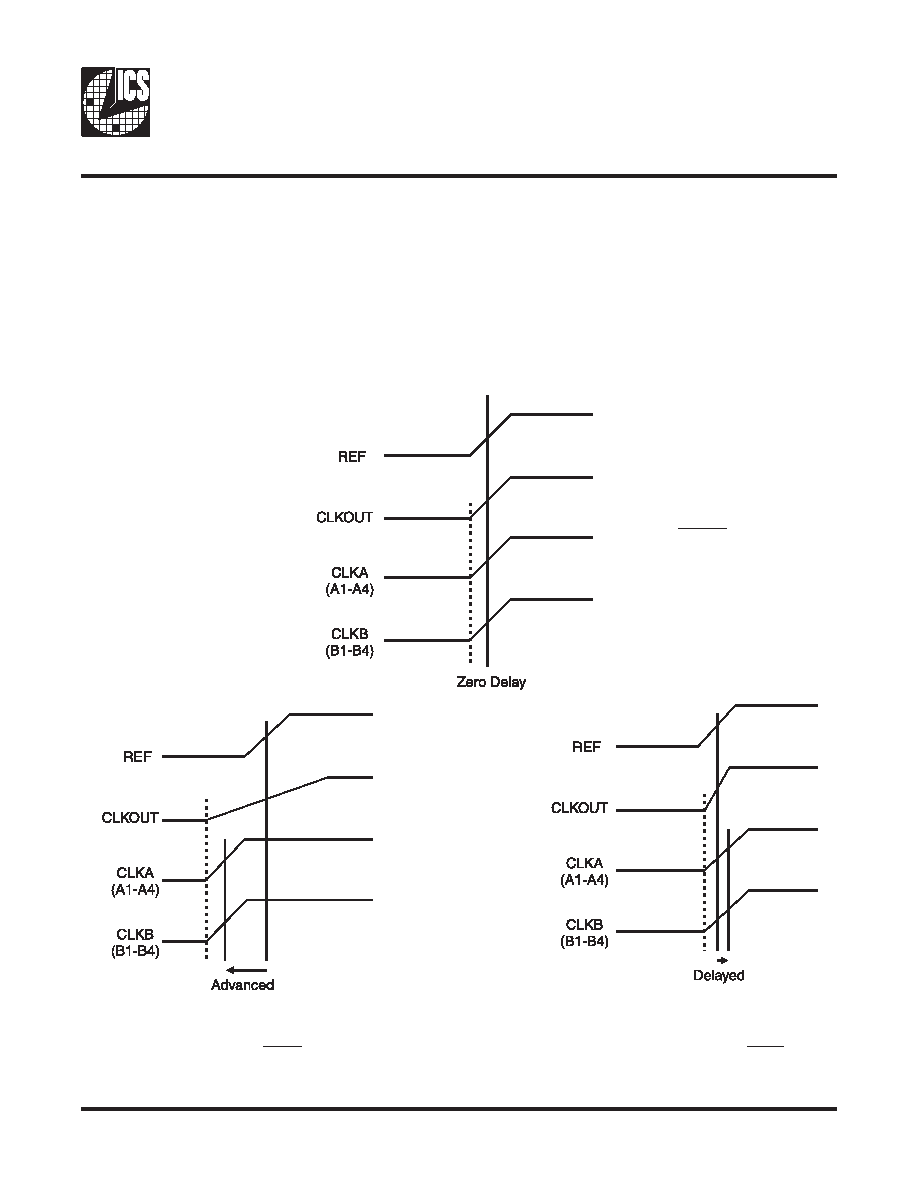
Output to Output Skew
The skew between CLKOUT and the CLKA/B outputs is not dynamically adjusted by the PLL. Since CLKOUT is one
of the inputs to the PLL, zero phase difference is maintained from REF to CLKOUT. If all outputs are equally loaded,
zero phase difference will maintained from REF to all outputs.
If applications requiring zero output-output skew, all the outputs must equally loaded.
If the CLKA/B outputs are less loaded than CLKOUT, CLKA/B outputs will lead it; and if the CLKA/B is more loaded
than CLKOUT, CLKA/B will lag the CLKOUT.
Since the CLKOUT and the CLKA/B outputs are identical, they all start at the same time, but different loads cause them
to have different rise times and different times crossing the measurement thresholds.
REF input and
all outputs
loaded Equally
REF input and CLKA/B
outputs loaded equally, with
CLKOUT loaded More.
REF input and CLKA/B
outputs loaded equally, with
CLKOUT loaded Less.
Timing diagrams with different loading configurations
相关PDF资料 |
PDF描述 |
|---|---|
| ICS9112YF-17-T | PLL BASED CLOCK DRIVER, 8 TRUE OUTPUT(S), 0 INVERTED OUTPUT(S), PDSO16 |
| ICS9112YM-26LF-T | LOW SKEW CLOCK DRIVER, 4 TRUE OUTPUT(S), 0 INVERTED OUTPUT(S), PDSO8 |
| ICS9112YM-26LFT | 9112 SERIES, LOW SKEW CLOCK DRIVER, 4 TRUE OUTPUT(S), 0 INVERTED OUTPUT(S), PDSO8 |
| ICS9112YM-28LF-T | 9112 SERIES, LOW SKEW CLOCK DRIVER, 5 TRUE OUTPUT(S), 0 INVERTED OUTPUT(S), PDSO8 |
| ICS9112YM-28LF-T | 9112 SERIES, LOW SKEW CLOCK DRIVER, 5 TRUE OUTPUT(S), 0 INVERTED OUTPUT(S), PDSO8 |
相关代理商/技术参数 |
参数描述 |
|---|---|
| ICS9112YM-27-T | 制造商:ICS 制造商全称:ICS 功能描述:Low Skew PCI / PCI-X Buffer |
| ICS9112YM-28LF-T | 制造商:ICS 制造商全称:ICS 功能描述:Low Skew Output Buffer |
| ICS9117-01 | 制造商:ICS 制造商全称:ICS 功能描述:Frequency Generator for Modem Systems |
| ICS9117M-01 | 制造商:ICS 制造商全称:ICS 功能描述:Frequency Generator for Modem Systems |
| ICS9117M02 | 制造商:未知厂家 制造商全称:未知厂家 功能描述:Peripheral IC |
发布紧急采购,3分钟左右您将得到回复。