- 您现在的位置:买卖IC网 > PDF目录61073 > ICS9147F-09LF (INTEGRATED DEVICE TECHNOLOGY INC) 83.3 MHz, PROC SPECIFIC CLOCK GENERATOR, PDSO48 PDF资料下载
参数资料
| 型号: | ICS9147F-09LF |
| 厂商: | INTEGRATED DEVICE TECHNOLOGY INC |
| 元件分类: | 时钟产生/分配 |
| 英文描述: | 83.3 MHz, PROC SPECIFIC CLOCK GENERATOR, PDSO48 |
| 封装: | SSOP-48 |
| 文件页数: | 6/9页 |
| 文件大小: | 580K |
| 代理商: | ICS9147F-09LF |
6
ICS9147-09
Pins 2, 15, 46 and 47 on the ICS9147-09 serve as dual
signal functions to the device. During initial power-up,
they act as input pins. The logic level (voltage) that is
present on these pins at this time is read and stored into a
4-bit internal data latch. At the end of Power-On reset, (see
AC characteristics for timing values), the device changes
the mode of operations for these pins to an output function.
In this mode the pins produce the specified buffered
clocks to external loads.
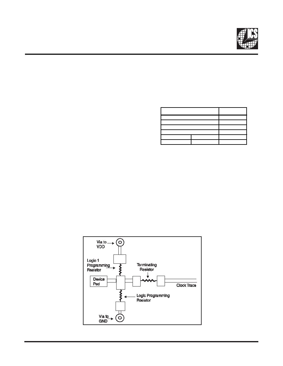
To program (load) the internal configuration register for
these pins, a resistor is connected to either theVDD (logic 1)
power supply or the GND (logic 0) voltage potential. A 10
Kilohm(10K) resistor is used to provide both the solid CMOS
programming voltage needed during the power-up
programming period and to provide an insignificant load on
the output clock during the subsequent operating period.
Figs. 1 and 2 show the recommended means of implementing
this function. In Fig. 1 either one of the resistors is loaded
onto the board (selective stuffing) to configure the devices
internal logic. Figs. 2a and b provide a single resistor
loading option where either solder spot tabs or a physical
jumper header may be used.
These figures illustrate the optimal PCB physical layout
options. These configuration resistors are of such a large
ohmic value that they do not effect the low impedance clock
signals. The layouts have been optimized to provide as little
impedance transition to the clock signal as possible, as it
passes through the programming resistor pad(s).
Shared Pin Operation -
Input/Output Pins
The ICS9147-09 includes a production test verification
mode of operation. This requires that the FS2 and FS1 pins
be programmed to a logic high and the FS0 pin be
programmed to a logic low(see Shared Pin Operation
section). In this mode the device will output the following
frequencies.
Note: REF is the frequency of either the crystal connected
between the devices X1and X2, or, in the case of a device
being driven by an external reference clock, the frequency
of the reference (or test) clock on the devices X1 pin.
Test Mode Operation
Fig. 1
Pin
Frequency
REF, IOAPIC
REF
48MHz
REF/2
24MHz
REF/4
CPU, SDRAM
REF2
BUS
BSEL=1
REF/4
BUS
BSEL=0
REF/3
相关PDF资料 |
PDF描述 |
|---|---|
| ICS9147F-09 | 83.3 MHz, PROC SPECIFIC CLOCK GENERATOR, PDSO48 |
| ICS9148F-13 | 100 MHz, PROC SPECIFIC CLOCK GENERATOR, PDSO48 |
| ICS9148F-PPP-LF | 100 MHz, PROC SPECIFIC CLOCK GENERATOR, PDSO48 |
| ICS9148F-49 | 100 MHz, PROC SPECIFIC CLOCK GENERATOR, PDSO28 |
| ICS9148F-49LF | 100 MHz, PROC SPECIFIC CLOCK GENERATOR, PDSO28 |
相关代理商/技术参数 |
参数描述 |
|---|---|
| ICS9147F-12 | 制造商:ICS 制造商全称:ICS 功能描述:Pentium/ProTM System and Cyrix⑩ Clock Chip |
| ICS9147F-14 | 制造商:ICS 制造商全称:ICS 功能描述:Frequency Generator & Integrated Buffers for PENTIUM/ProTM |
| ICS9147F-16 | 制造商:ICS 制造商全称:ICS 功能描述:Frequency Generator & Integrated Buffers for PENTIUMTM |
| ICS9147F-22 | 制造商:ICS 制造商全称:ICS 功能描述:Pentium/ProTM System and Cyrix™ Clock Chip |
| ICS9148-02 | 制造商:ICS 制造商全称:ICS 功能描述:Pentium/ProTM System Clock Chip |
发布紧急采购,3分钟左右您将得到回复。