- 您现在的位置:买卖IC网 > PDF目录67705 > ICS9148F-17 (INTEGRATED DEVICE TECHNOLOGY INC) 100.3569 MHz, PROC SPECIFIC CLOCK GENERATOR, PDSO48 PDF资料下载
参数资料
| 型号: | ICS9148F-17 |
| 厂商: | INTEGRATED DEVICE TECHNOLOGY INC |
| 元件分类: | 时钟产生/分配 |
| 英文描述: | 100.3569 MHz, PROC SPECIFIC CLOCK GENERATOR, PDSO48 |
| 封装: | 0.300 INCH, SSOP-48 |
| 文件页数: | 1/16页 |
| 文件大小: | 473K |
| 代理商: | ICS9148F-17 |
Integrated
Circuit
Systems, Inc.
General Description
Features
ICS9148-17
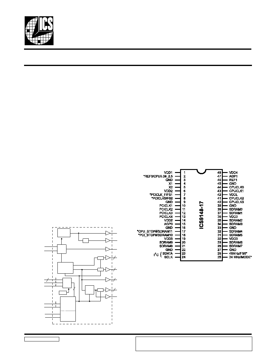
Block Diagram
Pentium is a trademark of Intel Corporation
I
2C is a trademark of Philips Corporation
Frequency Generator & Integrated Buffers for PENTIUM/ProTM
9148-17 Rev F 10/21/99
Pin Configuration
3.3Voutputs: SDRAM,AGP, PCI, REF, 48/24 MHz
2.5V or 3.3V outputs: CPU
20 ohm CPU clock output impedance
20 ohm PCI clock output impedance
CPU to PCI skew = 2 to 6ns
No external load cap for CL=18pF crystals
250 ps max CPU, PCI clock skew
Smooth CPU frequency transition among all CPU
frequencies.
I2C interface for programming
2ms power up clock stable time
Clock duty cycle 45-55%.
48 pin 300 mil SSOP package
3.3V operation, 5V tolerant inputs.
48-Pin SSOP
Power Groups
VDD1 = REF (0:1), X1, X2
VDD2 = PCICLK_F, PCICLK(0:5)
VDD3 = SDRAM (0:11), supply for PLL core,
24 MHz, 48MHz
VDD4=AGP(0:1)
VDDL=CPUCLK(0:3)
* Internal Pull-up Resistor of
240K to 3.3V on indicated inputs
The ICS9148-17 generates all clocks required for high speed
RISC or CISC microprocessor systems such as Intel PentiumPro
or Cyrix. Eight different reference frequency multiplying factors
are externally selectable with smooth frequency transitions.
Features include four CPU, six PCI, two AGP (=2xPCI) and
Twelve SDRAM clocks. Two reference outputs are available
equal to the crystal frequency. One 48 MHz for USB, and one
24 MHz clock for Super IO. Built in ±1.5%, 0.6% center or down
spread spectrum modulation to reduce EMI. Serial
programming I2C interface allows changing functions, stop
clock programing and frequency selection. Additionally, the
device meets the Pentium power-up stabilization, which
requires that CPU and PCI clocks be stable within 2ms after
power-up.
High drive PCICLK and SDRAM outputs typically provide
greater than 1 V/ns slew rate into 30pF loads. CPUCLK outputs
typically provide better than 1V/ns slew rate into 20pF loads
while maintaining 50±5% duty cycle. The REF and 24 and 48
MHz clock outputs typically provide better than 0.5V/ns slew
rates.
CPU_STOP#
PCI_STOP#
PLL2
PLL1
Spread
Spectrum
48MHz
24MHz
REF (0:1)
CPUCLK (0:3)
SDRAM (0:11)
PCICLK (0:4)
PCICLK_F
X1
X2
XTAL
OSC
PCI
CLOCK
DIVDER
STOP
SDATA
SCLK
FS(0:2)
MODE
CPU3.3#_2.5
Control
Logic
Config.
Reg.
AGP(0:1)
LATCH
POR
PCI_STOP
CPU_STOP
2
4
12
5
3
/2
ICS reserves the right to make changes in the device data identified in this
publication without further notice. ICS advises its customers to obtain the latest
version of all device data to verify that any information being relied upon by the
customer is current and accurate.
相关PDF资料 |
PDF描述 |
|---|---|
| ICS9148F-18LF | 100 MHz, PROC SPECIFIC CLOCK GENERATOR, PDSO28 |
| ICS9148F-25 | 83.3 MHz, PROC SPECIFIC CLOCK GENERATOR, PDSO48 |
| ICS9148F-32 | 100 MHz, PROC SPECIFIC CLOCK GENERATOR, PDSO48 |
| ICS9148F-58LF | 133.3 MHz, PROC SPECIFIC CLOCK GENERATOR, PDSO48 |
| ICS9148F-58LF | 133.3 MHz, PROC SPECIFIC CLOCK GENERATOR, PDSO48 |
相关代理商/技术参数 |
参数描述 |
|---|---|
| ICS9148F-18 | 制造商:ICS 制造商全称:ICS 功能描述:Pentium/ProTM System Clock Chip |
| ICS9148F-20 | 制造商:ICS 制造商全称:ICS 功能描述:Pentium/ProTM System Clock Chip |
| ICS9148F25 | 制造商:未知厂家 制造商全称:未知厂家 功能描述:Industrial Control IC |
| ICS9148F-25 | 功能描述:IC CLK SYNTHESIZER CHIP 48-SSOP RoHS:否 类别:集成电路 (IC) >> 时钟/计时 - 专用 系列:- 标准包装:28 系列:- 类型:时钟/频率发生器 PLL:是 主要目的:Intel CPU 服务器 输入:时钟 输出:LVCMOS 电路数:1 比率 - 输入:输出:3:22 差分 - 输入:输出:无/是 频率 - 最大:400MHz 电源电压:3.135 V ~ 3.465 V 工作温度:0°C ~ 85°C 安装类型:表面贴装 封装/外壳:64-TFSOP (0.240",6.10mm 宽) 供应商设备封装:64-TSSOP 包装:管件 |
| ICS9148F-25T | 功能描述:IC CLK SYNTHESIZER CHIP 48-SSOP RoHS:否 类别:集成电路 (IC) >> 时钟/计时 - 专用 系列:- 标准包装:28 系列:- 类型:时钟/频率发生器 PLL:是 主要目的:Intel CPU 服务器 输入:时钟 输出:LVCMOS 电路数:1 比率 - 输入:输出:3:22 差分 - 输入:输出:无/是 频率 - 最大:400MHz 电源电压:3.135 V ~ 3.465 V 工作温度:0°C ~ 85°C 安装类型:表面贴装 封装/外壳:64-TFSOP (0.240",6.10mm 宽) 供应商设备封装:64-TSSOP 包装:管件 |
发布紧急采购,3分钟左右您将得到回复。