- 您现在的位置:买卖IC网 > PDF目录67705 > ICS9148F-58LF 133.3 MHz, PROC SPECIFIC CLOCK GENERATOR, PDSO48 PDF资料下载
参数资料
| 型号: | ICS9148F-58LF |
| 元件分类: | 时钟产生/分配 |
| 英文描述: | 133.3 MHz, PROC SPECIFIC CLOCK GENERATOR, PDSO48 |
| 封装: | 0.300 INCH, SSOP-48 |
| 文件页数: | 9/14页 |
| 文件大小: | 449K |
| 代理商: | ICS9148F-58LF |
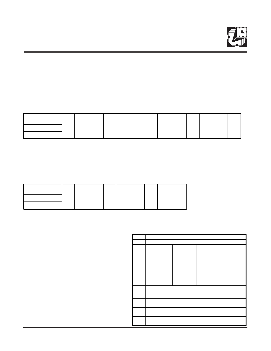
4
ICS9148- 58
Byte0: Functionality and Frequency Select Register
(default = 0)
Serial Configuration Command Bitmap
Bit
Description
PWD
Bit 7 Reserved
0
Bit
6:4
Bit6 Bit5
Bit4
111
110
101
100
011
010
001
000
CPU Clock
100.2
95.25
83.3
133.3
75
124
66.8
112
PCI
33.3
31.75
33.3
44.3
37.5
41.3
33.4
37.3
AGP
66.6
63.5
66.6
88.7
75
82.7
66.8
74.7
Note
1
Bit 3
0 - Frequency is selected by hardware select,
Latched Inputs
1 - Frequency is selected by Bit 6:4 (above)
0
Bit 2
0 - Spread Spectrum center spread type. ±.25%
1 - Spread Spectrum down spread type. 0 to -.5%
0
Bit 1 0 - Normal
1 - Spread Spectrum Enabled
0
Bit 0
0 - Running
1- Tristate all outputs
0
General I
2C serial interface information
The information in this section assumes familiarity with I2C programming. For more information, contact ICS for an I2C
programming application note.
How to Write:
Send the address D2(H) .
Send two additional dummy bytes, a command code
and byte count.
Send the desired number of data bytes.
See the diagram below:
Note that the acknowledge bit is sent by the clock chip, and pulls the data line low. There is no minimum of data bytes that must
be sent.
How to Read:
Send the address D3(H).
Send the byte count in binary coded decimal
Read back the desired number of data bytes
See the diagram below:
The following specifications should be observed:
1.
Operating voltage for I2C pins is 3.3V
2.
Maximum data transfer rate (SCLK) is 100K bits/sec.
Clock Generator
Address (7 bits)
ACK
+ 8 bits
dummy
command code
ACK
+ 8 bits
dummy Byte
count
ACK
Data Byte
1
ACK
Data Byte
N
ACK
A(6:0) & R/W#
D2(H)
Clock Generator
Address (7 bits)
ACK
Byte
C ount
ACK
Data Byte
1
AC K
Data Byte
N
A(6:0) & R/W#
D3(H)
I2C is a trademark of Philips Corporation
Note 1. Default at Power-up will be for latched logic inputs
to define frequency. Bits 4, 5, 6 are default to 000,
and if bit 3 is written to a 1 to use Bits 6:4, then
these should be defined to desired frequency at same
write cycle.
Note: PWD = Power-Up Default
相关PDF资料 |
PDF描述 |
|---|---|
| ICS9148F-58 | 133.3 MHz, PROC SPECIFIC CLOCK GENERATOR, PDSO48 |
| ICS9148F-93LF | 100 MHz, PROC SPECIFIC CLOCK GENERATOR, PDSO48 |
| ICS9148F-93 | 100 MHz, PROC SPECIFIC CLOCK GENERATOR, PDSO48 |
| ICS9148GF12-T | 66.6 MHz, PROC SPECIFIC CLOCK GENERATOR, PDSO48 |
| ICS9148YF-111LF | 100 MHz, PROC SPECIFIC CLOCK GENERATOR, PDSO48 |
相关代理商/技术参数 |
参数描述 |
|---|---|
| ICS9148F-60 | 制造商:未知厂家 制造商全称:未知厂家 功能描述:CPU System Clock Generator |
| ICS9148F-75-T | 制造商:ICS 制造商全称:ICS 功能描述:Frequency Generator & Integrated Buffers for Mother Boards |
| ICS9148F-PPP-T | 制造商:ICS 制造商全称:ICS 功能描述:Frequency Generator & Integrated Buffers for Mother Boards |
| ICS9148G-12 | 制造商:ICS 制造商全称:ICS 功能描述:Pentium/ProTM System Clock Chip |
| ICS9148M-46 | 制造商:未知厂家 制造商全称:未知厂家 功能描述:CPU System Clock Generator |
发布紧急采购,3分钟左右您将得到回复。