- 您现在的位置:买卖IC网 > PDF目录1999 > ICS951402AGLF (IDT, Integrated Device Technology Inc)IC TIMING CTRL HUB P4 48-TSSOP PDF资料下载
参数资料
| 型号: | ICS951402AGLF |
| 厂商: | IDT, Integrated Device Technology Inc |
| 文件页数: | 12/23页 |
| 文件大小: | 0K |
| 描述: | IC TIMING CTRL HUB P4 48-TSSOP |
| 标准包装: | 39 |
| 系列: | TCH™ |
| 类型: | 时钟/频率发生器,多路复用器 |
| PLL: | 是 |
| 主要目的: | Intel CPU,Timing Control Hub? |
| 输入: | 晶体 |
| 输出: | 时钟 |
| 电路数: | 1 |
| 比率 - 输入:输出: | 1:19 |
| 差分 - 输入:输出: | 无/是 |
| 频率 - 最大: | 210MHz |
| 电源电压: | 3.135 V ~ 3.465 V |
| 工作温度: | 0°C ~ 70°C |
| 安装类型: | 表面贴装 |
| 封装/外壳: | 48-TFSOP(0.240",6.10mm 宽) |
| 供应商设备封装: | 48-TSSOP |
| 包装: | 管件 |
| 其它名称: | 951402AGLF |
2
Integrated
Circuit
Systems, Inc.
ICS951402
Advance Information
0660—05/05/05
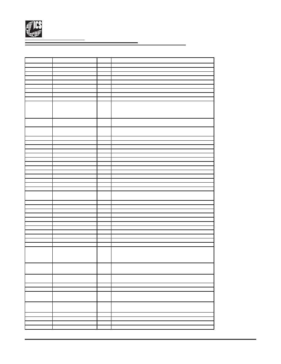
Pin Description
PIN NUMBER
PIN NAME
TYPE
DESCRIPTION
1
VDDREF
PWR
Ref, XTAL power supply, nominal 3.3V
2
FS0/REF0
I/O
Frequency select latch input pin / 14.318 MHz reference clock.
3
FS1/REF1
I/O
Frequency select latch input pin / 14.318 MHz reference clock.
4
FS2/REF2
I/O
Frequency select latch input pin / 14.318 MHz reference clock.
5
GNDREF
PWR
Ground pin for the REF outputs.
6
X1
IN
Crystal input, Nominally 14.318MHz.
7
X2
OUT
Crystal output, Nominally 14.318MHz
8
GND
PWR
Ground pin.
9
VDD
PWR
Power supply, nominal 3.3V
10
*VttPWR_GD/PD#
IN
This 3.3V LVTTL input is a level sensitive strobe used to determine
when latch inputs are valid and are ready to be sampled. This is an
active high input. / Asynchronous active low input pin used to power
down the device into a low power state.
11
PCI66/33#_SEL
IN
Selects all PCI clock frequencies to be 33Mhz or 66Mhz. 0 = 33Mhz , 1
= 66Mhz
12
PCI_STOP#*
IN
Stops all PCICLKs besides the PCICLK_F clocks at logic 0 level, when
input low
13
VDDPCI
PWR
Power supply for PCI clocks, nominal 3.3V
14
FS3/PCICLK_F0
I/O
Frequency select latch input pin / 3.3V PCI free running clock output.
15
FS4/PCICLK_F1
I/O
Frequency select latch input pin / 3.3V PCI free running clock output.
16
PCICLK0
OUT
PCI clock output.
17
PCICLK1
OUT
PCI clock output.
18
GNDPCI
PWR
Ground pin for the PCI outputs
19
VDDPCI
PWR
Power supply for PCI clocks, nominal 3.3V
20
PCICLK2
OUT
PCI clock output.
21
PCICLK3
OUT
PCI clock output.
22
PCICLK4
OUT
PCI clock output.
23
PCICLK5
OUT
PCI clock output.
24
GNDPCI
PWR
Ground pin for the PCI outputs
25
GND48
PWR
Ground pin for the 48MHz outputs
26
24_48MHz/SEL24_48#MHz**
I/O
24/48MHz clock output / Latched select input for 24/48MHz output.
0=48MHz, 1 = 24MHz.
27
48MHz_1
OUT
48MHz clock output.
28
48MHz_0
OUT
48MHz clock output.
29
AVDD48
PWR
Analog power for 48MHz outputs and fixed PLL core, nominal 3.3V
30
VDDAGP
PWR
Power supply for AGP clocks, nominal 3.3V
31
AGPCLK1
OUT
AGP clock output
32
AGPCLK0
OUT
AGP clock output
33
GNDAGP
PWR
Ground pin for the AGP outputs
34
SDATA
I/O
Data pin for SMBus circuitry, 5V tolerant.
35
SCLK
IN
Clock pin of SMBus circuitry, 5V tolerant.
36
AVDD
PWR
3.3V Analog Power pin for Core PLL
37
GND
PWR
Ground pin.
38
IREF
OUT
This pin establishes the reference current for the differential current-
mode output pairs. This pin requires a fixed precision resistor tied to
ground in order to establish the appropriate current. 475 ohms is the
standard value.
39
CPUCLKC0
OUT
Complementary clock of differential pair CPU outputs. This clock is 180
degrees out of phase with the SDRAM clock.
40
CPUCLKT0
OUT
True clock of differential pair CPU outputs. This clock is in phase with
the SDRAM clock
41
GNDCPU
PWR
Ground pin for the CPU outputs
42
VDDCPU
PWR
Supply for CPU clocks, 3.3V nominal
43
CPUCLKC1
OUT
Complementary clock of differential pair CPU outputs. This clock is 180
degrees out of phase with the SDRAM clock.
44
CPUCLKT1
OUT
True clock of differential pair CPU outputs. This clock is in phase with
the SDRAM clock
45
CPU_STOP#*
IN
Stops all CPUCLK besides the free running clocks
46
GNDSDR
PWR
Ground pin for the SDRAM outputs.
47
SDRAM_OUT
OUT
SDRAM seed clock output for external buffer
48
VDDSDR
PWR
Supply for SDRAM clocks, nominal 3.3V.
相关PDF资料 |
PDF描述 |
|---|---|
| ICS95V847AGIT | IC CLOCK DRIVER 2.5V 24-TSSOP |
| ICS95V850AGT | IC CLK DVR PLL 1:10 48TSSOP |
| ICS95V857ALT | IC CLK DVR PLL 1:10 40TVSOP |
| ICS95V857CKLF8 | IC CLK DVR PLL 1:10 40VFQFN |
| ICS97U870AKT | IC CLK DVR PLL 1:10 40VFQFN |
相关代理商/技术参数 |
参数描述 |
|---|---|
| ICS951402AGLFT | 功能描述:IC TIMING CTRL HUB P4 48-TSSOP RoHS:是 类别:集成电路 (IC) >> 时钟/计时 - 专用 系列:TCH™ 标准包装:28 系列:- 类型:时钟/频率发生器 PLL:是 主要目的:Intel CPU 服务器 输入:时钟 输出:LVCMOS 电路数:1 比率 - 输入:输出:3:22 差分 - 输入:输出:无/是 频率 - 最大:400MHz 电源电压:3.135 V ~ 3.465 V 工作温度:0°C ~ 85°C 安装类型:表面贴装 封装/外壳:64-TFSOP (0.240",6.10mm 宽) 供应商设备封装:64-TSSOP 包装:管件 |
| ICS951402YFLF-T | 制造商:ICS 制造商全称:ICS 功能描述:Programmable Timing Control Hub for P4 processor |
| ICS951402YGLF-T | 制造商:ICS 制造商全称:ICS 功能描述:Programmable Timing Control Hub for P4 processor |
| ICS951403 | 制造商:ICS 制造商全称:ICS 功能描述:AMD-K7 System Clock Chip |
| ICS951403YFLF-T | 制造商:ICS 制造商全称:ICS 功能描述:AMD-K7 System Clock Chip |
发布紧急采购,3分钟左右您将得到回复。