- 您现在的位置:买卖IC网 > PDF目录1999 > ICS95V850AGT (IDT, Integrated Device Technology Inc)IC CLK DVR PLL 1:10 48TSSOP PDF资料下载
参数资料
| 型号: | ICS95V850AGT |
| 厂商: | IDT, Integrated Device Technology Inc |
| 文件页数: | 10/10页 |
| 文件大小: | 0K |
| 描述: | IC CLK DVR PLL 1:10 48TSSOP |
| 产品变化通告: | Product Discontinuation 09/Dec/2011 |
| 标准包装: | 1,000 |
| 类型: | 时钟缓冲器/驱动器,多路复用器 |
| PLL: | 是 |
| 主要目的: | 存储器,DDR |
| 输入: | LVCMOS,LVDS,LVPELL,LVTTL |
| 输出: | SSTL-2 |
| 电路数: | 1 |
| 比率 - 输入:输出: | 1:10 |
| 差分 - 输入:输出: | 是/是 |
| 频率 - 最大: | 210MHz |
| 电源电压: | 2.3 V ~ 2.7 V |
| 工作温度: | 0°C ~ 85°C |
| 安装类型: | 表面贴装 |
| 封装/外壳: | 48-TFSOP(0.240",6.10mm 宽) |
| 供应商设备封装: | 48-TSSOP |
| 包装: | 带卷 (TR) |
| 其它名称: | 95V850AGT |
9
ICS95V850
0458G—11/21/08
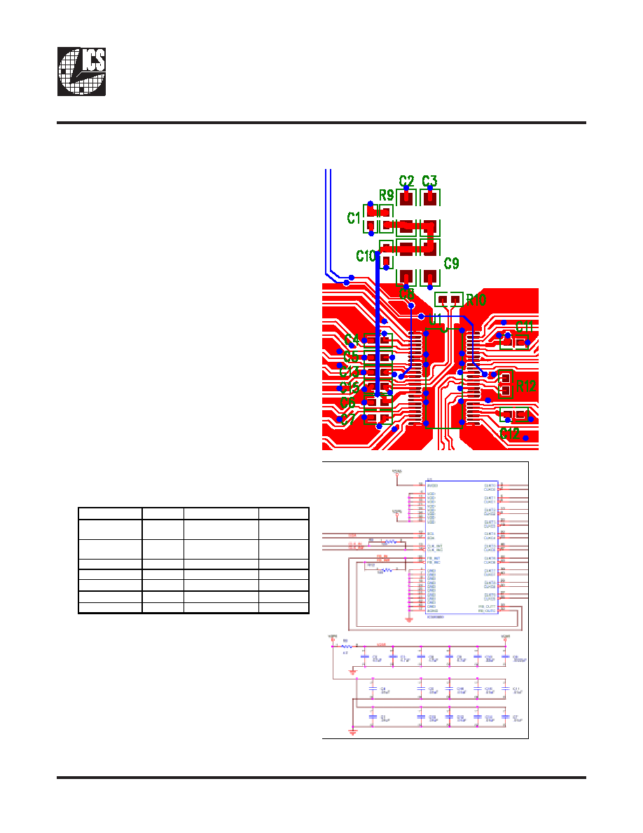
General Layout Precautions:
Use copper flooded ground on the top signal layer under the
clock buffer The area under U1 on the right is an example.
Flood over the ground vias.
1)
Use power vias for power and ground. Vias 20 mil or
larger in diameter have lower high frequency impedance.
Vias for signals may be minimum drill size.
2)
Make all power and ground traces are as wide as the via
pad for lower inductance.
3)
VAA for pin 16 has a low pass RC filter to decouple the
digital and analog supplies. The 4.7uF capacitors may be
replaced with a single low ESR device with the same
total capacitance. VAA is routed on a outside signal
layer. Do not cut a power or ground plane and route in it.
4)
Notice that ground vias are never shared.
5)
When ever possible, VCC (net V2P5 in the schematic)
pins have a decoupling capacitor. Power is always routed
from the plane connection via to the capacitor pad to the
VCC pin on the clock buffer. Moats or plane cuts are not
used to isolate power.
6)
Differential mode clock output traces are routed:
a.
With a ground trace between the pairs. Trace is
grounded on both ends.
b.
Without a ground trace, clock pairs are routed with a
separation of at least 5 times the thickness of the
dielectric. If the dielectric thickness is 4.5 mil, the
trace separation is at least 18 mils.
7) Terminate differential CLK_IN and FB_IN traces after
routing to buffer pads.
Component Values:
Ref Desg.
Value
Description
Package
C1,C4,C5,
C7,C11,C12
.01uF
CERAMIC MLC
0603
C2,C3,C8,
C9
4.7uF
CERAMIC MLC
1206
C10
.22uF
CERAMIC MLC
0603
C6
2200pF
CERAMIC MLC
0603
R9,R12
120
0603
R9
4.7
0603
U1
ICS95V850
TSSOP48
Recommended Layout for the ICS95V850
相关PDF资料 |
PDF描述 |
|---|---|
| ICS95V857ALT | IC CLK DVR PLL 1:10 40TVSOP |
| ICS95V857CKLF8 | IC CLK DVR PLL 1:10 40VFQFN |
| ICS97U870AKT | IC CLK DVR PLL 1:10 40VFQFN |
| ICS97ULP877AHT | IC CLOCK DRIVER 1.8V LP 52-BGA |
| ICS97ULP877BKLFT | IC CLOCK DRIVER 1.8V LP 40VFQFPN |
相关代理商/技术参数 |
参数描述 |
|---|---|
| ICS95V857 | 制造商:ICSI 制造商全称:Integrated Circuit Solution Inc 功能描述:2.5V Wide Range Frequency Clock Driver (45MHz - 233MHz) |
| ICS95V857_09 | 制造商:ICS 制造商全称:ICS 功能描述:2.5V Wide Range Frequency Clock Driver (45MHz - 233MHz) |
| ICS95V857AG | 功能描述:IC CLK DVR PLL 1:10 48TSSOP RoHS:否 类别:集成电路 (IC) >> 时钟/计时 - 专用 系列:- 标准包装:28 系列:- 类型:时钟/频率发生器 PLL:是 主要目的:Intel CPU 服务器 输入:时钟 输出:LVCMOS 电路数:1 比率 - 输入:输出:3:22 差分 - 输入:输出:无/是 频率 - 最大:400MHz 电源电压:3.135 V ~ 3.465 V 工作温度:0°C ~ 85°C 安装类型:表面贴装 封装/外壳:64-TFSOP (0.240",6.10mm 宽) 供应商设备封装:64-TSSOP 包装:管件 |
| ICS95V857AG-130LF-T | 制造商:ICSI 制造商全称:Integrated Circuit Solution Inc 功能描述:2.5V Wide Range Frequency Clock Driver (45MHz - 233MHz) |
| ICS95V857AGILF | 功能描述:IC CLK DVR PLL 1:10 48TSSOP RoHS:是 类别:集成电路 (IC) >> 时钟/计时 - 专用 系列:- 标准包装:28 系列:- 类型:时钟/频率发生器 PLL:是 主要目的:Intel CPU 服务器 输入:时钟 输出:LVCMOS 电路数:1 比率 - 输入:输出:3:22 差分 - 输入:输出:无/是 频率 - 最大:400MHz 电源电压:3.135 V ~ 3.465 V 工作温度:0°C ~ 85°C 安装类型:表面贴装 封装/外壳:64-TFSOP (0.240",6.10mm 宽) 供应商设备封装:64-TSSOP 包装:管件 |
发布紧急采购,3分钟左右您将得到回复。