- 您现在的位置:买卖IC网 > PDF目录67709 > ICS9DB106YG-T (INTEGRATED DEVICE TECHNOLOGY INC) 9DB SERIES, PLL BASED CLOCK DRIVER, 3 TRUE OUTPUT(S), 0 INVERTED OUTPUT(S), PDSO28 PDF资料下载
参数资料
| 型号: | ICS9DB106YG-T |
| 厂商: | INTEGRATED DEVICE TECHNOLOGY INC |
| 元件分类: | 时钟及定时 |
| 英文描述: | 9DB SERIES, PLL BASED CLOCK DRIVER, 3 TRUE OUTPUT(S), 0 INVERTED OUTPUT(S), PDSO28 |
| 封装: | 4.40 MM, 0.65 MM PITCH, MO-153, TSSOP-28 |
| 文件页数: | 7/14页 |
| 文件大小: | 164K |
| 代理商: | ICS9DB106YG-T |
2
Integrated
Circuit
Systems, Inc.
ICS9DB106
0833C—08/17/06
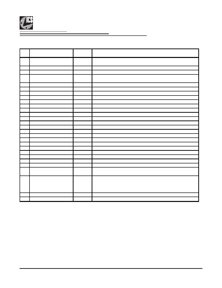
Pin Description
PIN #
PIN NAME
PIN TYPE
DESCRIPTION
1
PLL_BW
IN
3.3V input for selecting PLL Band Width
0 = low, 1= high
2
CLK_INT
IN
"True" reference clock input.
3
CLK_INC
IN
"Complimentary" reference clock input.
4
**CLKREQ1#
IN
Output enable for PCI Express output pair '1'
0 = enabled, 1 = tri-stated
5
PCIEXT0
OUT
True clock of differential PCI_Express pair.
6
PCIEXC0
OUT
Complement clock of differential PCI_Express pair.
7
VDD
PWR
Power supply, nominal 3.3V
8
GND
IN
Ground pin.
9
PCIEXT1
OUT
True clock of differential PCI_Express pair.
10
PCIEXC1
OUT
Complement clock of differential PCI_Express pair.
11
PCIEXT2
OUT
True clock of differential PCI_Express pair.
12
PCIEXC2
OUT
Complement clock of differential PCI_Express pair.
13
VDD
PWR
Power supply, nominal 3.3V
14
SMBDAT
I/O
Data pin of SMBUS circuitry, 5V tolerant
15
SMBCLK
IN
Clock pin of SMBUS circuitry, 5V tolerant
16
VDD
PWR
Power supply, nominal 3.3V
17
PCIEXC3
OUT
Complement clock of differential PCI_Express pair.
18
PCIEXT3
OUT
True clock of differential PCI_Express pair.
19
PCIEXC4
OUT
Complement clock of differential PCI_Express pair.
20
PCIEXT4
OUT
True clock of differential PCI_Express pair.
21
GND
PWR
Ground pin.
22
VDD
PWR
Power supply, nominal 3.3V
23
PCIEXC5
OUT
Complement clock of differential PCI_Express pair.
24
PCIEXT5
OUT
True clock of differential PCI_Express pair.
25
**CLKREQ4#
IN
Output enable for PCI Express output pair '4'
0 = enabled, 1 = tri-stated
26
IREF
OUT
This pin establishes the reference current for the differential current-
mode output pairs. This pin requires a fixed precision resistor tied to
ground in order to establish the appropriate current. 475 ohms is the
standard value.
27
GNDA
PWR
Ground pin for the PLL core.
28
VDDA
PWR
3.3V power for the PLL core.
Note:
Pins preceeded by '**' have internal 120K ohm pull down resistors
相关PDF资料 |
PDF描述 |
|---|---|
| ICS9DB106YGLFT | 9DB SERIES, PLL BASED CLOCK DRIVER, 3 TRUE OUTPUT(S), 0 INVERTED OUTPUT(S), PDSO28 |
| ICS9DB106YFLFT | 9DB SERIES, PLL BASED CLOCK DRIVER, 3 TRUE OUTPUT(S), 0 INVERTED OUTPUT(S), PDSO28 |
| ICS9DB108YGLFT | 9DB SERIES, PLL BASED CLOCK DRIVER, 8 TRUE OUTPUT(S), 0 INVERTED OUTPUT(S), PDSO48 |
| ICS9DB108YFT | 9DB SERIES, PLL BASED CLOCK DRIVER, 8 TRUE OUTPUT(S), 0 INVERTED OUTPUT(S), PDSO48 |
| ICS9DB108YGT | 9DB SERIES, PLL BASED CLOCK DRIVER, 8 TRUE OUTPUT(S), 0 INVERTED OUTPUT(S), PDSO48 |
相关代理商/技术参数 |
参数描述 |
|---|---|
| ICS9DB108BF | 制造商:ICS 功能描述: |
| ICS9DB108BFLF | 功能描述:IC BUFFER 8OUTPUT DIFF 48-SSOP RoHS:是 类别:集成电路 (IC) >> 时钟/计时 - 专用 系列:PCI Express® (PCIe) 标准包装:1 系列:- 类型:时钟/频率发生器,多路复用器 PLL:是 主要目的:存储器,RDRAM 输入:晶体 输出:LVCMOS 电路数:1 比率 - 输入:输出:1:2 差分 - 输入:输出:无/是 频率 - 最大:400MHz 电源电压:3 V ~ 3.6 V 工作温度:0°C ~ 85°C 安装类型:表面贴装 封装/外壳:16-TSSOP(0.173",4.40mm 宽) 供应商设备封装:16-TSSOP 包装:Digi-Reel® 其它名称:296-6719-6 |
| ICS9DB108BFLFT | 功能描述:IC BUFFER 8OUTPUT DIFF 48-SSOP RoHS:是 类别:集成电路 (IC) >> 时钟/计时 - 专用 系列:PCI Express® (PCIe) 标准包装:28 系列:- 类型:时钟/频率发生器 PLL:是 主要目的:Intel CPU 服务器 输入:时钟 输出:LVCMOS 电路数:1 比率 - 输入:输出:3:22 差分 - 输入:输出:无/是 频率 - 最大:400MHz 电源电压:3.135 V ~ 3.465 V 工作温度:0°C ~ 85°C 安装类型:表面贴装 封装/外壳:64-TFSOP (0.240",6.10mm 宽) 供应商设备封装:64-TSSOP 包装:管件 |
| ICS9DB108BG | 制造商:INT_CIR_SYS 功能描述: |
| ICS9DB108BGLF | 功能描述:IC BUFFER 8OUTPUT DIFF 48-TSSOP RoHS:是 类别:集成电路 (IC) >> 时钟/计时 - 专用 系列:PCI Express® (PCIe) 标准包装:1 系列:- 类型:时钟/频率发生器,多路复用器 PLL:是 主要目的:存储器,RDRAM 输入:晶体 输出:LVCMOS 电路数:1 比率 - 输入:输出:1:2 差分 - 输入:输出:无/是 频率 - 最大:400MHz 电源电压:3 V ~ 3.6 V 工作温度:0°C ~ 85°C 安装类型:表面贴装 封装/外壳:16-TSSOP(0.173",4.40mm 宽) 供应商设备封装:16-TSSOP 包装:Digi-Reel® 其它名称:296-6719-6 |
发布紧急采购,3分钟左右您将得到回复。