- 您现在的位置:买卖IC网 > PDF目录8751 > IDT5T905PGGI (IDT, Integrated Device Technology Inc)IC CLK BUFF 1:5 250MHZ 28-TSSOP PDF资料下载
参数资料
| 型号: | IDT5T905PGGI |
| 厂商: | IDT, Integrated Device Technology Inc |
| 文件页数: | 13/19页 |
| 文件大小: | 0K |
| 描述: | IC CLK BUFF 1:5 250MHZ 28-TSSOP |
| 标准包装: | 50 |
| 类型: | 扇出缓冲器(分配) |
| 电路数: | 1 |
| 比率 - 输入:输出: | 1:5 |
| 差分 - 输入:输出: | 是/无 |
| 输入: | eHSTL,HSTL,LVPECL,LVTTL |
| 输出: | eHSTL,HSTL,LVTTL |
| 频率 - 最大: | 250MHz |
| 电源电压: | 2.4 V ~ 2.6 V |
| 工作温度: | -40°C ~ 85°C |
| 安装类型: | 表面贴装 |
| 封装/外壳: | 28-TSSOP(0.173",4.40mm 宽) |
| 供应商设备封装: | 28-TSSOP |
| 包装: | 管件 |
| 其它名称: | 5T905PGGI 800-2433-5 IDT5T905PGGI-ND |
INDUSTRIALTEMPERATURERANGE
IDT5T905
2.5VSINGLEDATARATE1:5CLOCKBUFFERTERABUFFER
3
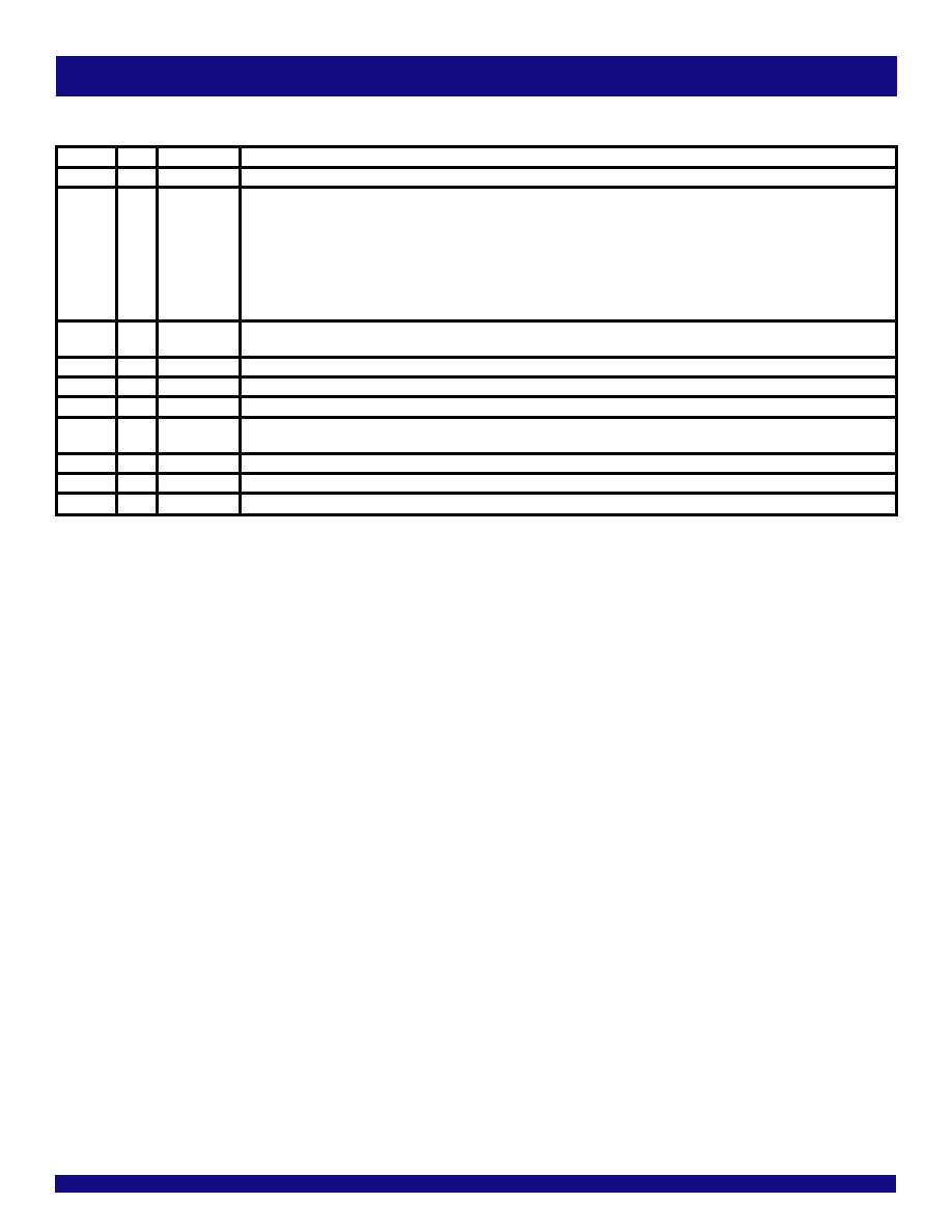
PIN DESCRIPTION
Symbol
I/O
Type
Description
A
I
Adjustable(1)
Clock input. A is the "true" side of the differential clock input. If operating in single-ended mode, A is the clock input.
A
/VREF
I
Adjustable(1)
Complementary clock input. A/VREF is the "complementary" side of A if the input is in differential mode. If operating in single-ended
mode, A/VREF is connected to GND. For single-ended operation in differential mode, A/VREF should be set to the desired toggle
voltage for A:
2.5VLVTTL
VREF = 1250mV
1.8V LVTTL, eHSTL
VREF = 900mV
HSTL
VREF = 750mV
LVEPECL
VREF = 1082mV
G
I
LVTTL(5)
Gate control for Qn outputs. When G is LOW, these outputs are enabled. When G is HIGH, these outputs are asynchronously
disabled to the level designated by GL(4).
GL
I
LVTTL(5)
Specifies output disable level. If HIGH, the outputs disable HIGH. If LOW, the outputs disable LOW.
Qn
O
Adjustable(2)
Clockoutputs
RxS
I
3 Level(3)
Selects single-ended 2.5V LVTTL (HIGH), 1.8V LVTTL (MID) clock input or differential (LOW) clock input
TxS
I
3 Level(3)
Sets the drive strength of the output drivers to be 2.5V LVTTL (HIGH), 1.8V LVTTL (MID) or HSTL (LOW) compatible. Used in
conjunction with VDDQtosettheinterfacelevels.
VDD
PWR
Power supply for the device core and inputs
VDDQ
PWR
Power supply for the device outputs. When utilizing 2.5V LVTTL outputs, VDDQ should be connected to VDD.
GND
PWR
Power supply return for all power
NOTES:
1. Inputs are capable of translating the following interface standards. User can select between:
Single-ended 2.5V LVTTL levels
Single-ended 1.8V LVTTL levels
or
Differential 2.5V/1.8V LVTTL levels
Differential HSTL and eHSTL levels
Differential LVEPECL levels
2. Outputs are user selectable to drive 2.5V, 1.8V LVTTL, eHSTL, or HSTL interface levels when used with the appropriate VDDQ voltage.
3. 3 level inputs are static inputs and must be tied to VDD or GND or left floating. These inputs are not hot-insertable or over-voltage tolerant.
4. Because the gate controls are asynchronous, runt pulses are possible. It is the user's responsibility to either time the gate control signals to minimize the possibility of runt
pulses or be able to tolerate them in down stream circuitry.
5. Pins listed as LVTTL inputs will accept 2.5V signals when RxS = HIGH or 1.8V signals when RxS = LOW or MID.
相关PDF资料 |
PDF描述 |
|---|---|
| VE-26V-MW-F1 | CONVERTER MOD DC/DC 5.8V 100W |
| VE-25X-MW-F4 | CONVERTER MOD DC/DC 5.2V 100W |
| VE-25X-MW-F2 | CONVERTER MOD DC/DC 5.2V 100W |
| VE-JNH-MZ-F3 | CONVERTER MOD DC/DC 52V 25W |
| VE-25X-MW-F1 | CONVERTER MOD DC/DC 5.2V 100W |
相关代理商/技术参数 |
参数描述 |
|---|---|
| IDT5T905PGGI8 | 功能描述:IC CLK BUFF 1:5 250MHZ 28-TSSOP RoHS:是 类别:集成电路 (IC) >> 时钟/计时 - 时钟缓冲器,驱动器 系列:- 标准包装:74 系列:- 类型:扇出缓冲器(分配) 电路数:1 比率 - 输入:输出:1:10 差分 - 输入:输出:是/是 输入:HCSL, LVCMOS, LVDS, LVPECL, LVTTL 输出:HCSL,LVDS 频率 - 最大:400MHz 电源电压:3 V ~ 3.6 V 工作温度:-40°C ~ 85°C 安装类型:表面贴装 封装/外壳:32-VFQFN 裸露焊盘 供应商设备封装:32-QFN(5x5) 包装:管件 |
| IDT5T905PGI | 功能描述:IC CLK BUFF 1:5 250MHZ 28-TSSOP RoHS:否 类别:集成电路 (IC) >> 时钟/计时 - 时钟缓冲器,驱动器 系列:- 标准包装:74 系列:- 类型:扇出缓冲器(分配) 电路数:1 比率 - 输入:输出:1:10 差分 - 输入:输出:是/是 输入:HCSL, LVCMOS, LVDS, LVPECL, LVTTL 输出:HCSL,LVDS 频率 - 最大:400MHz 电源电压:3 V ~ 3.6 V 工作温度:-40°C ~ 85°C 安装类型:表面贴装 封装/外壳:32-VFQFN 裸露焊盘 供应商设备封装:32-QFN(5x5) 包装:管件 |
| IDT5T9070PAGI | 功能描述:IC CLK BUFF 1:10 200MHZ 48-TSSOP RoHS:是 类别:集成电路 (IC) >> 时钟/计时 - 时钟缓冲器,驱动器 系列:TeraBuffer™ JR 产品培训模块:High Bandwidth Product Overview 标准包装:1,000 系列:Precision Edge® 类型:扇出缓冲器(分配) 电路数:1 比率 - 输入:输出:1:4 差分 - 输入:输出:是/是 输入:CML,LVDS,LVPECL 输出:CML 频率 - 最大:2.5GHz 电源电压:2.375 V ~ 2.625 V 工作温度:-40°C ~ 85°C 安装类型:表面贴装 封装/外壳:16-VFQFN 裸露焊盘,16-MLF? 供应商设备封装:16-MLF?(3x3) 包装:带卷 (TR) |
| IDT5T9070PAGI8 | 功能描述:IC CLK BUFF 1:10 200MHZ 48-TSSOP RoHS:是 类别:集成电路 (IC) >> 时钟/计时 - 时钟缓冲器,驱动器 系列:TeraBuffer™ JR 标准包装:74 系列:- 类型:扇出缓冲器(分配) 电路数:1 比率 - 输入:输出:1:10 差分 - 输入:输出:是/是 输入:HCSL, LVCMOS, LVDS, LVPECL, LVTTL 输出:HCSL,LVDS 频率 - 最大:400MHz 电源电压:3 V ~ 3.6 V 工作温度:-40°C ~ 85°C 安装类型:表面贴装 封装/外壳:32-VFQFN 裸露焊盘 供应商设备封装:32-QFN(5x5) 包装:管件 |
| IDT5T907PAGI | 功能描述:IC CLK BUFF 1:10 250MHZ 48-TSSOP RoHS:是 类别:集成电路 (IC) >> 时钟/计时 - 时钟缓冲器,驱动器 系列:TeraBuffer™ 标准包装:74 系列:- 类型:扇出缓冲器(分配) 电路数:1 比率 - 输入:输出:1:10 差分 - 输入:输出:是/是 输入:HCSL, LVCMOS, LVDS, LVPECL, LVTTL 输出:HCSL,LVDS 频率 - 最大:400MHz 电源电压:3 V ~ 3.6 V 工作温度:-40°C ~ 85°C 安装类型:表面贴装 封装/外壳:32-VFQFN 裸露焊盘 供应商设备封装:32-QFN(5x5) 包装:管件 |
发布紧急采购,3分钟左右您将得到回复。