- 您现在的位置:买卖IC网 > PDF目录8751 > IDT5T905PGGI (IDT, Integrated Device Technology Inc)IC CLK BUFF 1:5 250MHZ 28-TSSOP PDF资料下载
参数资料
| 型号: | IDT5T905PGGI |
| 厂商: | IDT, Integrated Device Technology Inc |
| 文件页数: | 16/19页 |
| 文件大小: | 0K |
| 描述: | IC CLK BUFF 1:5 250MHZ 28-TSSOP |
| 标准包装: | 50 |
| 类型: | 扇出缓冲器(分配) |
| 电路数: | 1 |
| 比率 - 输入:输出: | 1:5 |
| 差分 - 输入:输出: | 是/无 |
| 输入: | eHSTL,HSTL,LVPECL,LVTTL |
| 输出: | eHSTL,HSTL,LVTTL |
| 频率 - 最大: | 250MHz |
| 电源电压: | 2.4 V ~ 2.6 V |
| 工作温度: | -40°C ~ 85°C |
| 安装类型: | 表面贴装 |
| 封装/外壳: | 28-TSSOP(0.173",4.40mm 宽) |
| 供应商设备封装: | 28-TSSOP |
| 包装: | 管件 |
| 其它名称: | 5T905PGGI 800-2433-5 IDT5T905PGGI-ND |
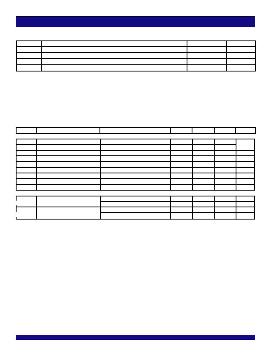
INDUSTRIALTEMPERATURERANGE
6
IDT5T905
2.5VSINGLEDATARATE1:5CLOCKBUFFERTERABUFFER
DIFFERENTIAL INPUT AC TEST CONDITIONS FOR HSTL
Symbol
Parameter
Value
Units
VDIF
Input Signal Swing(1)
1V
VX
DifferentialInputSignalCrossingPoint(2)
750
mV
VTHI
InputTimingMeasurementReferenceLevel(3)
CrossingPoint
V
tR, tF
InputSignalEdgeRate(4)
1
V/ns
NOTES:
1. The 1V peak-to-peak input pulse level is specified to allow consistent, repeatable results in an automatic test equipment (ATE) environment. Compliant devices must meet the
VDIF (AC) specification under actual use conditions.
2. A 750mV crossing point level is specified to allow consistent, repeatable results in an automatic test equipment (ATE) environment. Compliant devices must meet the VX specification
under actual use conditions.
3. In all cases, input waveform timing is marked at the differential cross-point of the input signals.
4. The input signal edge rate of 1V/ns or greater is to be maintained in the 20% to 80% range of the input waveform.
DC ELECTRICAL CHARACTERISTICS OVER OPERATING RANGE FOR eHSTL(1)
Symbol
Parameter
Test Conditions
Min.
Typ.(7)
Max
Unit
InputCharacteristics
IIH
Input HIGH Current(9)
VDD = 2.6V
VI = VDDQ/GND
—
±5
μA
IIL
InputLOWCurrent(9)
VDD = 2.6V
VI = GND/VDDQ
——
±5
VIK
ClampDiodeVoltage
VDD = 2.4V, IIN = -18mA
—
- 0.7
- 1.2
V
VIN
DCInputVoltage
- 0.3
+3.6
V
VDIF
DCDifferentialVoltage(2,8)
0.2
—
V
VCM
DC Common Mode Input Voltage(3,8)
800
900
1000
mV
VIH
DC Input HIGH(4,5,8)
VREF + 100
—
mV
VIL
DC Input LOW(4,6,8)
—VREF - 100
mV
VREF
Single-EndedReferenceVoltage(4,8)
—
900
—
mV
OutputCharacteristics
VOH
Output HIGH Voltage
IOH = -8mA
VDDQ - 0.4
—
V
IOH = -100
μAVDDQ - 0.1
—
V
VOL
OutputLOWVoltage
IOL = 8mA
—
0.4
V
IOL = 100
μA
—
0.1
V
NOTES:
1. See RECOMMENDED OPERATING RANGE table.
2. VDIF specifies the minimum input differential voltage (VTR - VCP) required for switching where VTR is the "true" input level and VCP is the "complement" input level. Differential mode
only. The DC differential voltage must be maintained to guarantee retaining the existing HIGH or LOW input. The AC differential voltage must be achieved to guarantee switching
to a new state.
3. VCM specifies the maximum allowable range of (VTR + VCP) /2. Differential mode only.
4. For single-ended operation, in a differential mode, A/VREF is tied to the DC voltage VREF.
5. Voltage required to maintain a logic HIGH, single-ended operation in differential mode.
6. Voltage required to maintain a logic LOW, single-ended operation in differential mode.
7. Typical values are at VDD = 2.5V, VDDQ = 1.8V, +25°C ambient.
8. The reference clock input is capable of HSTL, eHSTL, LVEPECL, 1.8V or 2.5V LVTTL operation independent of the device output. The correct input interface table should be
referenced.
9. For differential mode (RxS = LOW), A and A/VREF must be at the opposite rail.
相关PDF资料 |
PDF描述 |
|---|---|
| VE-26V-MW-F1 | CONVERTER MOD DC/DC 5.8V 100W |
| VE-25X-MW-F4 | CONVERTER MOD DC/DC 5.2V 100W |
| VE-25X-MW-F2 | CONVERTER MOD DC/DC 5.2V 100W |
| VE-JNH-MZ-F3 | CONVERTER MOD DC/DC 52V 25W |
| VE-25X-MW-F1 | CONVERTER MOD DC/DC 5.2V 100W |
相关代理商/技术参数 |
参数描述 |
|---|---|
| IDT5T905PGGI8 | 功能描述:IC CLK BUFF 1:5 250MHZ 28-TSSOP RoHS:是 类别:集成电路 (IC) >> 时钟/计时 - 时钟缓冲器,驱动器 系列:- 标准包装:74 系列:- 类型:扇出缓冲器(分配) 电路数:1 比率 - 输入:输出:1:10 差分 - 输入:输出:是/是 输入:HCSL, LVCMOS, LVDS, LVPECL, LVTTL 输出:HCSL,LVDS 频率 - 最大:400MHz 电源电压:3 V ~ 3.6 V 工作温度:-40°C ~ 85°C 安装类型:表面贴装 封装/外壳:32-VFQFN 裸露焊盘 供应商设备封装:32-QFN(5x5) 包装:管件 |
| IDT5T905PGI | 功能描述:IC CLK BUFF 1:5 250MHZ 28-TSSOP RoHS:否 类别:集成电路 (IC) >> 时钟/计时 - 时钟缓冲器,驱动器 系列:- 标准包装:74 系列:- 类型:扇出缓冲器(分配) 电路数:1 比率 - 输入:输出:1:10 差分 - 输入:输出:是/是 输入:HCSL, LVCMOS, LVDS, LVPECL, LVTTL 输出:HCSL,LVDS 频率 - 最大:400MHz 电源电压:3 V ~ 3.6 V 工作温度:-40°C ~ 85°C 安装类型:表面贴装 封装/外壳:32-VFQFN 裸露焊盘 供应商设备封装:32-QFN(5x5) 包装:管件 |
| IDT5T9070PAGI | 功能描述:IC CLK BUFF 1:10 200MHZ 48-TSSOP RoHS:是 类别:集成电路 (IC) >> 时钟/计时 - 时钟缓冲器,驱动器 系列:TeraBuffer™ JR 产品培训模块:High Bandwidth Product Overview 标准包装:1,000 系列:Precision Edge® 类型:扇出缓冲器(分配) 电路数:1 比率 - 输入:输出:1:4 差分 - 输入:输出:是/是 输入:CML,LVDS,LVPECL 输出:CML 频率 - 最大:2.5GHz 电源电压:2.375 V ~ 2.625 V 工作温度:-40°C ~ 85°C 安装类型:表面贴装 封装/外壳:16-VFQFN 裸露焊盘,16-MLF? 供应商设备封装:16-MLF?(3x3) 包装:带卷 (TR) |
| IDT5T9070PAGI8 | 功能描述:IC CLK BUFF 1:10 200MHZ 48-TSSOP RoHS:是 类别:集成电路 (IC) >> 时钟/计时 - 时钟缓冲器,驱动器 系列:TeraBuffer™ JR 标准包装:74 系列:- 类型:扇出缓冲器(分配) 电路数:1 比率 - 输入:输出:1:10 差分 - 输入:输出:是/是 输入:HCSL, LVCMOS, LVDS, LVPECL, LVTTL 输出:HCSL,LVDS 频率 - 最大:400MHz 电源电压:3 V ~ 3.6 V 工作温度:-40°C ~ 85°C 安装类型:表面贴装 封装/外壳:32-VFQFN 裸露焊盘 供应商设备封装:32-QFN(5x5) 包装:管件 |
| IDT5T907PAGI | 功能描述:IC CLK BUFF 1:10 250MHZ 48-TSSOP RoHS:是 类别:集成电路 (IC) >> 时钟/计时 - 时钟缓冲器,驱动器 系列:TeraBuffer™ 标准包装:74 系列:- 类型:扇出缓冲器(分配) 电路数:1 比率 - 输入:输出:1:10 差分 - 输入:输出:是/是 输入:HCSL, LVCMOS, LVDS, LVPECL, LVTTL 输出:HCSL,LVDS 频率 - 最大:400MHz 电源电压:3 V ~ 3.6 V 工作温度:-40°C ~ 85°C 安装类型:表面贴装 封装/外壳:32-VFQFN 裸露焊盘 供应商设备封装:32-QFN(5x5) 包装:管件 |
发布紧急采购,3分钟左右您将得到回复。