- 您现在的位置:买卖IC网 > PDF目录3975 > IDT70V7599S166BC8 (IDT, Integrated Device Technology Inc)IC SRAM 4MBIT 166MHZ 256BGA PDF资料下载
参数资料
| 型号: | IDT70V7599S166BC8 |
| 厂商: | IDT, Integrated Device Technology Inc |
| 文件页数: | 19/22页 |
| 文件大小: | 0K |
| 描述: | IC SRAM 4MBIT 166MHZ 256BGA |
| 标准包装: | 1,000 |
| 格式 - 存储器: | RAM |
| 存储器类型: | SRAM - 双端口,同步 |
| 存储容量: | 4.5M(128K x 36) |
| 速度: | 166MHz |
| 接口: | 并联 |
| 电源电压: | 3.15 V ~ 3.45 V |
| 工作温度: | 0°C ~ 70°C |
| 封装/外壳: | 256-LBGA |
| 供应商设备封装: | 256-CABGA(17x17) |
| 包装: | 带卷 (TR) |
| 其它名称: | 70V7599S166BC8 |
�� �
�
�IDT70V7599S�
�High-Speed� 128K� x� 36� Synchronous� Bank-Switchable� Dual-Port� Static� RAM�
�Industrial� and� Commercial� Temperature� Ranges�
�Functional� Description�
�The� IDT70V7599� is� a� high-speed� 128Kx36� (4� Mbit)� synchronous�
�Bank-Switchable� Dual-Ported� SRAM� organized� into� 64� independent�
�2Kx36� banks.� Based� on� a� standard� SRAM� core� instead� of� a� traditional� true�
�dual-port� memory� core,� this� bank-switchable� device� offers� the� benefits� of�
�increased� density� and� lower� cost-per-bit� while� retaining� many� of� the�
�features� of� true� dual-ports.� These� features� include� simultaneous,� random�
�access� to� the� shared� array,� separate� clocks� per� port,� 166� MHz� operating�
�speed,� full-boundary� counters,� and� pinouts� compatible� with� the� IDT70V3599�
�(128Kx36)� dual-port� family.�
�The� two� ports� are� permitted� independent,� simultaneous� access� into�
�separate� banks� within� the� shared� array.� Access� by� the� ports� into� specific�
�banks� are� controlled� by� the� bank� address� pins� under� the� user's� direct�
�control:� each� port� can� access� any� bank� of� memory� with� the� shared� array�
�that� is� not� currently� being� accessed� by� the� opposite� port� (i.e.,� BA� 0L� -� BA� 5L�
�≠� BA� 0R� -� BA� 5R� ).� In� the� event� that� both� ports� try� to� access� the� same� bank�
�at� the� same� time,� neither� access� will� be� valid,� and� data� at� the� two� specific�
�addresses� targeted� by� the� ports� within� that� bank� may� be� corrupted� (in� the�
�case� that� either� or� both� ports� are� writing)� or� may� result� in� invalid� output� (in�
�the� case� that� both� ports� are� trying� to� read).�
�The� IDT70V7599� provides� a� true� synchronous� Dual-Port� Static� RAM�
�BA� 6� (1)�
�interface.� Registered� inputs� provide� minimal� setup� and� hold� times� on�
�address,� data� and� all� critical� control� inputs.�
�An� asynchronous� output� enable� is� provided� to� ease� asynchronous�
�bus� interfacing.� Counter� enable� inputs� are� also� provided� to� stall� the�
�operation� of� the� address� counters� for� fast� interleaved� memory� applications.�
�A� HIGH� on� CE� 0� or� a� LOW� on� CE� 1� for� one� clock� cycle� will� power� down�
�the� internal� circuitry� on� each� port� (individually� controlled)� to� reduce� static�
�power� consumption.� Dual� chip� enables� allow� easier� banking� of� multiple�
�IDT70V7599S� for� depth� expansion� configurations.� Two� cycles� are�
�required� with� CE� 0� LOW� and� CE� 1� HIGH� to� read� valid� data� on� the� outputs.�
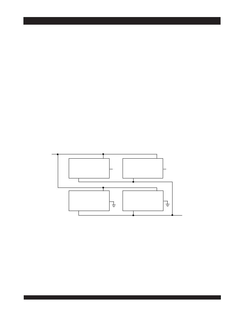
�Depth� and� Width� Expansion�
�The� IDT70V7599� features� dual� chip� enables� (refer� to� Truth�
�Table� I)� in� order� to� facilitate� rapid� and� simple� depth� expansion� with� no�
�requirements� for� external� logic.� Figure� 4� illustrates� how� to� control� the�
�various� chip� enables� in� order� to� expand� two� devices� in� depth.�
�The� IDT70V7599� can� also� be� used� in� applications� requiring� expanded�
�width,� as� indicated� in� Figure� 4.� Through� combining� the� control� signals,� the�
�devices� can� be� grouped� as� necessary� to� accommodate� applications�
�needing� 72-bits� or� wider.�
�IDT70V7599�
�CE� 0�
�IDT70V7599�
�CE� 0�
�Control� Inputs�
�CE� 1�
�V� DD�
�Control� Inputs�
�CE� 1�
�V� DD�
�IDT70V7599�
�CE� 1�
�IDT70V7599�
�CE� 1�
�Control� Inputs�
�CE� 0�
�Control� Inputs�
�CE� 0�
�BE� ,�
�R/� W� ,�
�OE� ,�
�CLK,�
�Figure� 4.� Depth� and� Width� Expansion� with� IDT70V7599�
�5626� drw� 20�
�ADS� ,�
�REPEAT� ,�
�CNTEN�
�,�
�NOTE:�
�1.� In� the� case� of� depth� expansion,� the� additional� address� pin� logically� serves� as� an� extension� of� the� bank� address.� Accesses� by� the� ports� into� specific� banks� are�
�controlled� by� the� bank� address� pins� under� the� user's� direct� control:� each� port� can� access� any� bank� of� memory� within� the� shared� array� that� is� not� currently�
�being� accessed� by� the� opposite� port� (i.e.,� BA� 0L� -� BA� 6L� ≠� BA� 0R� -� BA� 6R� ).� In� the� event� that� both� ports� try� to� access� the� same� bank� at� the� same� time,� neither�
�access� will� be� valid,� and� data� at� the� two� specific� addresses� targeted� by� the� parts� within� that� bank� may� be� corrupted� (in� the� case� that� either� or� both� parts� are�
�writing)� or� may� result� in� invalid� output� (in� the� case� that� both� ports� are� trying� to� read).�
�19�
�6.42�
�相关PDF资料 |
PDF描述 |
|---|---|
| IDT70V7319S166BF8 | IC SRAM 4MBIT 166MHZ 208FBGA |
| IDT70V7319S166BC8 | IC SRAM 4MBIT 166MHZ 256BGA |
| IDT70V658S10BFG8 | IC SRAM 2MBIT 10NS 208FBGA |
| IDT70V658S10BF8 | IC SRAM 2MBIT 10NS 208FBGA |
| IDT70V658S10BC8 | IC SRAM 2MBIT 10NS 256BGA |
相关代理商/技术参数 |
参数描述 |
|---|---|
| IDT70V7599S166BCI | 功能描述:IC SRAM 4MBIT 166MHZ 256BGA RoHS:否 类别:集成电路 (IC) >> 存储器 系列:- 标准包装:3,000 系列:- 格式 - 存储器:EEPROMs - 串行 存储器类型:EEPROM 存储容量:8K (1K x 8) 速度:400kHz 接口:I²C,2 线串口 电源电压:1.7 V ~ 5.5 V 工作温度:-40°C ~ 85°C 封装/外壳:8-SOIC(0.154",3.90mm 宽) 供应商设备封装:8-SOIC 包装:带卷 (TR) |
| IDT70V7599S166BCI8 | 功能描述:IC SRAM 4MBIT 166MHZ 256BGA RoHS:否 类别:集成电路 (IC) >> 存储器 系列:- 标准包装:3,000 系列:- 格式 - 存储器:EEPROMs - 串行 存储器类型:EEPROM 存储容量:8K (1K x 8) 速度:400kHz 接口:I²C,2 线串口 电源电压:1.7 V ~ 5.5 V 工作温度:-40°C ~ 85°C 封装/外壳:8-SOIC(0.154",3.90mm 宽) 供应商设备封装:8-SOIC 包装:带卷 (TR) |
| IDT70V7599S166BF | 功能描述:IC SRAM 4MBIT 166MHZ 208FBGA RoHS:否 类别:集成电路 (IC) >> 存储器 系列:- 标准包装:3,000 系列:- 格式 - 存储器:EEPROMs - 串行 存储器类型:EEPROM 存储容量:8K (1K x 8) 速度:400kHz 接口:I²C,2 线串口 电源电压:1.7 V ~ 5.5 V 工作温度:-40°C ~ 85°C 封装/外壳:8-SOIC(0.154",3.90mm 宽) 供应商设备封装:8-SOIC 包装:带卷 (TR) |
| IDT70V7599S166BF8 | 功能描述:IC SRAM 4MBIT 166MHZ 208FBGA RoHS:否 类别:集成电路 (IC) >> 存储器 系列:- 标准包装:3,000 系列:- 格式 - 存储器:EEPROMs - 串行 存储器类型:EEPROM 存储容量:8K (1K x 8) 速度:400kHz 接口:I²C,2 线串口 电源电压:1.7 V ~ 5.5 V 工作温度:-40°C ~ 85°C 封装/外壳:8-SOIC(0.154",3.90mm 宽) 供应商设备封装:8-SOIC 包装:带卷 (TR) |
| IDT70V7599S166DR | 功能描述:IC SRAM 4MBIT 166MHZ 208QFP RoHS:否 类别:集成电路 (IC) >> 存储器 系列:- 标准包装:3,000 系列:- 格式 - 存储器:EEPROMs - 串行 存储器类型:EEPROM 存储容量:8K (1K x 8) 速度:400kHz 接口:I²C,2 线串口 电源电压:1.7 V ~ 5.5 V 工作温度:-40°C ~ 85°C 封装/外壳:8-SOIC(0.154",3.90mm 宽) 供应商设备封装:8-SOIC 包装:带卷 (TR) |
发布紧急采购,3分钟左右您将得到回复。