- 您现在的位置:买卖IC网 > PDF目录9951 > IDT723651L20PQF (IDT, Integrated Device Technology Inc)IC FIFO SYNC 2048X36 132QFP PDF资料下载
参数资料
| 型号: | IDT723651L20PQF |
| 厂商: | IDT, Integrated Device Technology Inc |
| 文件页数: | 16/21页 |
| 文件大小: | 0K |
| 描述: | IC FIFO SYNC 2048X36 132QFP |
| 标准包装: | 36 |
| 系列: | 7200 |
| 功能: | 同步 |
| 存储容量: | 72K(2K x 36) |
| 数据速率: | 50MHz |
| 访问时间: | 20ns |
| 电源电压: | 4.5 V ~ 5.5 V |
| 工作温度: | 0°C ~ 70°C |
| 安装类型: | 表面贴装 |
| 封装/外壳: | 132-BQFP 缓冲式 |
| 供应商设备封装: | 132-PQFP(24.13x24.13) |
| 包装: | 托盘 |
| 其它名称: | 723651L20PQF |
4
COMMERCIALANDINDUSTRIAL
TEMPERATURERANGES
IDT723631/723641/723651 CMOS SyncFIFO
512 x 36, 1,024 x 36 and 2,048 x 36
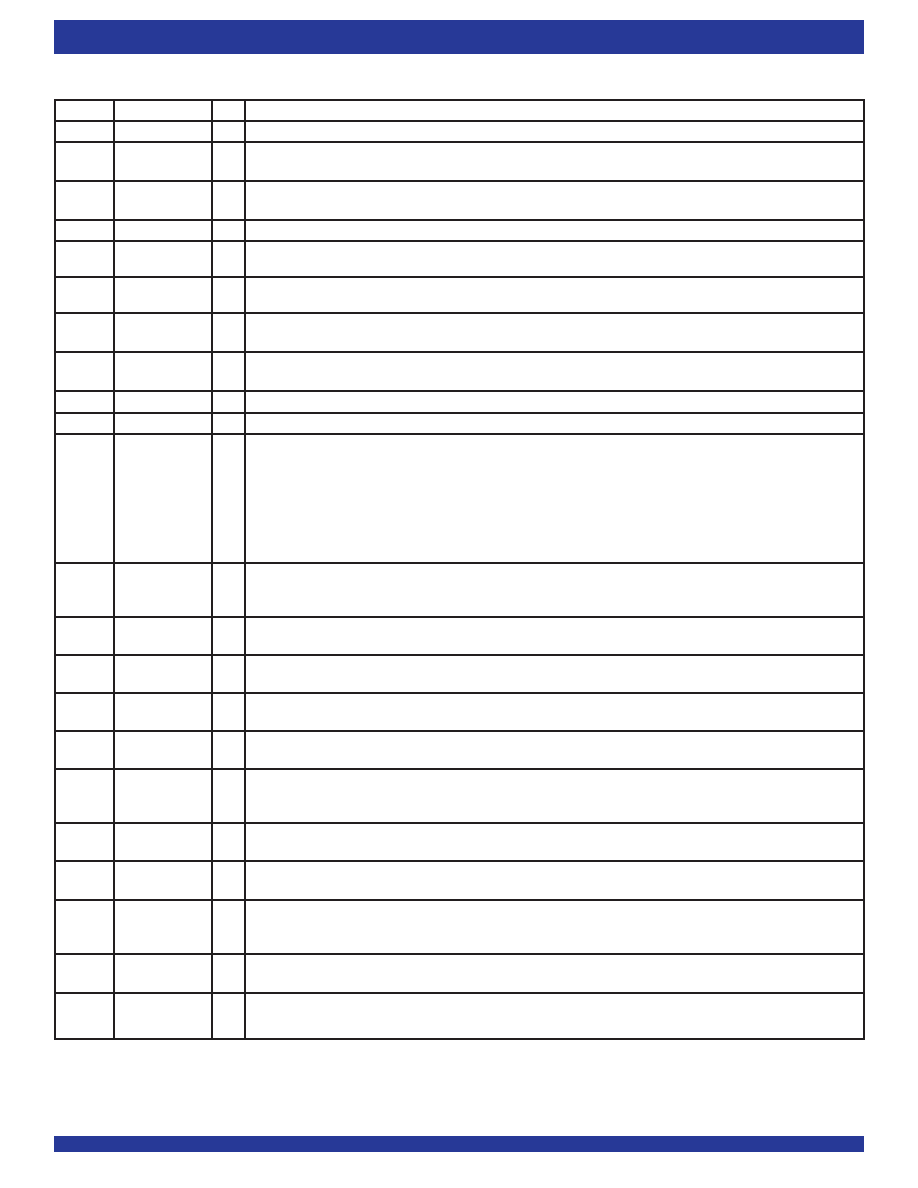
PIN DESCRIPTION
Symbol
Name
I/O
Description
A0-A35
Port-A Data
I/O
36-bit bidirectional data port for side A.
AE
Almost-Empty
O
Programmable flag synchronized to CLKB. It is LOW when the number of words in the FIFO is less than or equal to the value in
Flag
the Almost-Empty register (X).
AF
Almost-Full
O
Programmable flag synchronized to CLKA. It is LOW when the number of empty locations in FIFO is less than or equal to the
Flag
value in the Almost-Full Offset register (Y).
B0-B35
Port-B Data
I/O
36-bit bidirectional data port for side B.
CLKA
Port-A Clock
I
CLKA is a continuous clock that synchronizes all data transfers through port-A and may be asynchronous or coincident to CLKB.
IR and
AF are synchronous to the LOW-to-HIGH transition of CLKA.
CLKB
Port-B Clock
I
CLKB is a continuous clock that synchronizes all data transfers through port-B and may be asynchronous or coincident to CLKA.
OR and
AE are synchronous to the LOW-to-HIGH transition of CLKB.
CSA
Port-A Chip
I
CSA must be LOW to enable a LOW-to-HIGH transition of CLKA to read or write data on port-A. The A0-A35 outputs are in the
Select
high-impedance state when
CSA is HIGH.
CSB
Port-B Chip
I
CSB must be LOW to enable a LOW-to-HIGH transition of CLKB to read or write data on port-B. The B0-B35 outputs are in the
Select
high-impedance state when
CSB is HIGH.
ENA
Port-A Enable
I
ENA must be HIGH to enable a LOW-to-HIGH transition of CLKA to read or write data on port-A.
ENB
Port-B Enable
I
ENB must be HIGH to enable a LOW-to-HIGH transition of CLKB to read or write data on port-B.
FS1/
Flag-Offset
I
FS1/
SEN and FS0/SD are dual-purpose inputs used for flag Offset register programming. During a device reset, FS1/SEN and
SEN,
Select 1/
FS0/SD selects the flag offset programming method. Three Offset register programming methods are available: automatically
Serial Enable
load one of two preset values, parallel load from port A, and serial load.
FS0/SD
Flag Offset 0/
When serial load is selected for flag Offset register programming, FS1/
SENis used as an enable synchronous to the LOW-to-
Serial Data
HIGH transition of CLKA. When FS1/
SEN is LOW, a rising edge on CLKA load the bit present on FS0/SD into the X and Y
registers. The number of bit writes required to program the Offset registers is 18/20/22. The first bit write stores the Y-register
MSB and the last bit write stores the X-register LSB.
IR
Input Ready
O
IR is synchronized to the LOW-to-HIGH transition of CLKA. When IR is LOW, the FIFO is full and writes to its array are
Flag
disabled. When the FIFO is in retransmit mode, IR indicates when the memory has been filled to the point of the retransmit
data and prevents further writes. IR is set LOW during reset and is set HIGH after reset.
MBA
Port-A Mailbox
I
A HIGH level chooses a mailbox register for a port-A read or write operation.
Select
MBB
Port-B Mailbox
I
A HIGH level chooses a mailbox register for a port-B read or write operation. When the B0-B35 outputs are active, a HIGH
Select
level on MBB selects data from the mail1 register for output and a LOW level selects FIFO data for output.
MBF1
Mail1 Register
O
MBF1 is set LOW by the LOW-to-HIGH transition of CLKA that writes data to the mail1 register. MBF1 is set HIGH by a
Flag
LOW-to-HIGH transition of CLKB when a port-B readis selected and MBB is HIGH.
MBF1 is set HIGH by a reset.
MBF2
Mail2 Register
O
MBF2 is set LOW by the LOW-to-HIGH transition of CLKB that writes data to the mail2 register. MBF2 is set HIGH by a
Flag
LOW-to-HIGH transition of CLKA when a port-A read is selected and MBA is HIGH.
MBF2 is set HIGH by a reset.
OR
Output Ready
O
OR is synchronized to the LOW-to-HIGH transition of CLKB. When OR is LOW, the FIFO is empty and reads are disabled.
Flag
Ready data is present in the output register of the FIFO when OR is HIGH. OR is forced LOW during the reset and goes
HIGH on the third LOW-to-HIGH transition of CLKB after a word is loaded to empty memory.
RFM
Read From
I
When the FIFO is in retransmit mode, a HIGH on RFM enables a LOW-to-HIGH transition of CLKB to reset the read pointer
Mark
tothebeginningretransmitlocationandoutputthefirstselectedretransmitdata.
RST
Reset
I
To reset the device, four LOW-to-HIGH transitions of CLKA and four LOW-to-HIGH transitions of CLKB must occur while
RST
is LOW. The LOW-to-HIGH transition of
RST latches the status of FS0 and FS1 for AF and AE offset selection.
RTM
Retransmit
I
When RTM is HIGH and valid data is present in the FIFO output register (OR is HIGH), a LOW-to-HIGH transition of CLKB
Mode
selects the data for the beginning of a retransmit and puts the FIFO in retransmit mode. The selected word remains the initial
retransmit point until a LOW- to-HIGH transition of CLKB occurs while RTM is LOW, taking the FIFO out of retransmit mode.
W/
RA
Port-A Write/
I
A HIGH selects a write operation and a LOW selects a read operation on port A for a LOW-to-HIGH transition of CLKA. The
Read Select
A0-A35 outputs are in the high-impedance state when W/
RA is HIGH.
W/RB
Port-B Write/
I
A LOW selects a write operation and a HIGH selects a read operation on port B for a LOW-to-HIGH transition of CLKB. The
Read Select
B0-B35 outputs are in the high-impedance state when
W/RB is LOW.
相关PDF资料 |
PDF描述 |
|---|---|
| IDT723663L15PF | IC FIFO SYNC 4096X36 128QFP |
| MS27484T18B35SA | CONN PLUG 66POS STRAIGHT W/SCKT |
| IDT72605L20PF | IC FIFO BI SYNC 256X18 64-TQFP |
| MS3100F20-11P | CONN RCPT 13POS WALL MNT W/PINS |
| MS27468T15A97S | CONN RCPT 12POS JAM NUT W/SCKT |
相关代理商/技术参数 |
参数描述 |
|---|---|
| IDT723651L20PQFI | 功能描述:IC FIFO SYNC 2048X36 132QFP RoHS:否 类别:集成电路 (IC) >> 逻辑 - FIFO 系列:7200 标准包装:15 系列:74F 功能:异步 存储容量:256(64 x 4) 数据速率:- 访问时间:- 电源电压:4.5 V ~ 5.5 V 工作温度:0°C ~ 70°C 安装类型:通孔 封装/外壳:24-DIP(0.300",7.62mm) 供应商设备封装:24-PDIP 包装:管件 其它名称:74F433 |
| IDT723652L12PF | 功能描述:IC FIFO BI SYNC 4096X36 120QFP RoHS:否 类别:集成电路 (IC) >> 逻辑 - FIFO 系列:7200 标准包装:15 系列:74F 功能:异步 存储容量:256(64 x 4) 数据速率:- 访问时间:- 电源电压:4.5 V ~ 5.5 V 工作温度:0°C ~ 70°C 安装类型:通孔 封装/外壳:24-DIP(0.300",7.62mm) 供应商设备封装:24-PDIP 包装:管件 其它名称:74F433 |
| IDT723652L12PF8 | 功能描述:IC FIFO BI SYNC 4096X36 120QFP RoHS:否 类别:集成电路 (IC) >> 逻辑 - FIFO 系列:7200 标准包装:15 系列:74F 功能:异步 存储容量:256(64 x 4) 数据速率:- 访问时间:- 电源电压:4.5 V ~ 5.5 V 工作温度:0°C ~ 70°C 安装类型:通孔 封装/外壳:24-DIP(0.300",7.62mm) 供应商设备封装:24-PDIP 包装:管件 其它名称:74F433 |
| IDT723652L12PQF | 功能描述:IC FIFO BI SYNC 4096X36 132QFP RoHS:否 类别:集成电路 (IC) >> 逻辑 - FIFO 系列:7200 标准包装:15 系列:74F 功能:异步 存储容量:256(64 x 4) 数据速率:- 访问时间:- 电源电压:4.5 V ~ 5.5 V 工作温度:0°C ~ 70°C 安装类型:通孔 封装/外壳:24-DIP(0.300",7.62mm) 供应商设备封装:24-PDIP 包装:管件 其它名称:74F433 |
| IDT723652L15PF | 功能描述:IC FIFO BI SYNC 4096X36 120QFP RoHS:否 类别:集成电路 (IC) >> 逻辑 - FIFO 系列:7200 标准包装:15 系列:74F 功能:异步 存储容量:256(64 x 4) 数据速率:- 访问时间:- 电源电压:4.5 V ~ 5.5 V 工作温度:0°C ~ 70°C 安装类型:通孔 封装/外壳:24-DIP(0.300",7.62mm) 供应商设备封装:24-PDIP 包装:管件 其它名称:74F433 |
发布紧急采购,3分钟左右您将得到回复。