- 您现在的位置:买卖IC网 > PDF目录9994 > IDT72605L25J8 (IDT, Integrated Device Technology Inc)IC FIFO BI SYNC 256X18 68-PLCC PDF资料下载
参数资料
| 型号: | IDT72605L25J8 |
| 厂商: | IDT, Integrated Device Technology Inc |
| 文件页数: | 11/17页 |
| 文件大小: | 0K |
| 描述: | IC FIFO BI SYNC 256X18 68-PLCC |
| 标准包装: | 250 |
| 系列: | 7200 |
| 功能: | 同步 |
| 存储容量: | 9.2K(512 x 18) |
| 数据速率: | 40MHz |
| 访问时间: | 25ns |
| 电源电压: | 4.5 V ~ 5.5 V |
| 工作温度: | 0°C ~ 70°C |
| 安装类型: | 表面贴装 |
| 封装/外壳: | 68-LCC(J 形引线) |
| 供应商设备封装: | 68-PLCC(24x24) |
| 包装: | 带卷 (TR) |
| 其它名称: | 72605L25J8 |
3
IDT72605/72615 CMOS SYNCBiFIFO
256 x 18x 2 and 512 x 18 x 2
INDUSTRIALTEMPERATURERANGE
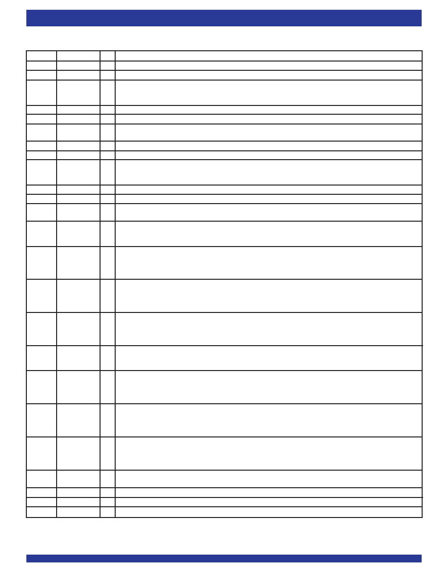
PIN DESCRIPTION
Symbol
Name
I/O
Description
DA0-DA17
Data A
I/O Data inputs & outputs for the 18-bit Port A bus.
CSA
Chip Select A
I
Port A is accessed when CSA is LOW. Port A is inactive if CSA is HIGH.
R/WA
Read/WriteA
I
This pin controls the read or write direction of Port A. If R/WA is LOW, Data A input data is written into Port A. If R/WA is HIGH,
Data A output data is read from Port A. In bypass mode, when R/WA is LOW, message is written into A
→B output register. If
R/WA is HIGH, message is read from B
→A output register.
CLKA
Clock A
I
CLKA is typically a free running clock. Data is read or written into Port A on the rising edge of CLKA.
ENA
Enable A
I
When ENA is LOW, data can be read or written to Port A. When ENA is HIGH, no data transfers occur.
OEA
Output Enable A
I
When R/WA is HIGH, Port A is an output bus and OEA controls the high-impedance state of DA0-DA17. If OEA is HIGH, Port A is
in a high-impedance state. If OEA is LOW while CSA is LOW and R/WA is HIGH, Port A is in an active (low-impedance) state.
A0, A1, A2 Addresses
I
When CSA is asserted, A0, A1, A2 and R/WA are used to select one of six internal resources.
DB0-DB17
Data B
I/O Data inputs & outputs for the 18-bit Port B bus.
R/WB
Read/WriteB
I
This pin controls the read or write direction of Port B. If R/WB is LOW, Data B input data is written into Port B. If R/WB is HIGH,
Data B output data is read from Port B. In bypass mode, when R/WB is LOW, message is written into B
→A output register. If
R/WB is HIGH, message is read from A
→B output register.
CLKB
Clock B
I
Clock B is typically a free running clock. Data is read or written into Port B on the rising edge of CLKB.
ENB
Enable B
I
When ENB is LOW, data can be read or written to Port B. When ENB is HIGH, no data transfers occur.
OEB
Output Enable B
I
When R/WB is HIGH, Port B is an output bus and OEB controls the high-impedance state of DB0-DB17. If OEB is HIGH, Port B is
in a high-impedance state. If OEB is LOW while R/WB is HIGH, Port B is in an active (low-impedance) state.
EFAB
A
→B Empty
O
When EFAB is LOW, the A
→B FIFO is empty and further data reads from Port B are inhibited. When EFAB is HIGH, the FIFO is
Flag
not empty. EFAB is synchronized to CLKB. In the bypass mode, EFAB HIGH indicates that data DA0-DA17 is available for passing
through. After the data DB0-DB17 has been read, EFAB goes LOW.
PAEAB
A
→B
O
When PAEAB is LOW, the A
→B FIFO is almost-empty. An almost-empty FIFO contains less than or equal to the offset
Programmable
programmed into PAEAB Register. When PAEAB is HIGH, the A
→B FIFO contains more than offset in PAEAB Register. The
Almost-Empty
default offset value for PAEAB Register is 8. PAEAB is synchronized to CLKB.
Flag
PAFAB
A
→B
O
When PAFAB is LOW, the A
→B FIFO is almost-full. An almost-full FIFO contains greater than the FIFO depth minus the offset
Programmable
programmed into PAFAB Register. When PAFAB is HIGH, the A
→B FIFO contains less than or equal to the depth minus the
Almost-Full
offset in PAFAB Register. The default offset value for PAFAB Register is 8. PAFAB is synchronized to CLKA.
Flag
FFAB
A
→B Full Flag
O
When FFAB is LOW, the A
→B FIFO is full and further data writes into Port A are inhibited. When FFAB is HIGH, the FIFO is not
full. FFAB is synchronized to CLKA. In bypass mode, FFAB tells Port A that a message is waiting in Port B’s output register. If
FFAB is LOW, a bypass message is in the register. If FFAB is HIGH, Port B has read the message and another message can be
written into Port A.
EFBA
B
→A Empty
O
When EFBA is LOW, the B
→A FIFO is empty and further data reads from Port A are inhibited. When EFBA is HIGH, the FIFO
Flag
is not empty. EFBA is synchronized to CLKA. In the bypass mode, EFBA HIGH indicates that data DB0-DB17 is available for
passing through. After the data DA0-DA17 has been read, EFBA goes LOW on the following cycle.
PAEBA
B
→A
O
When PAEBA is LOW, the B
→A FIFO is almost-empty. An almost-empty FIFO contains less than or equal to the offset
Programmable
programmed into PAEBA Register. When PAEBA is HIGH, the B
→A FIFO contains more than offset in PAEBA Register. The
Almost-Empty
default offset value for PAEBA Register is 8. PAEBA is synchronized to CLKA.
Flag
PAFBA
B
→A
O
When PAFBA is LOW, the B
→A FIFO is almost-full. An almost-full FIFO contains greater than the FIFO depth minus the offset
Programmable
programmed into PAFBA Register. When PAFBA is HIGH, the B
→A FIFO contains less than or equal to the depth minus the
Almost-Full
offset in PAFBA Register. The default offset value for PAFBA Register is 8. PAFBA is synchronized to CLKB.
Flag
FFBA
B
→A Full Flag
O
When FFBA is LOW, the B
→A FIFO is full and further data writes into Port B are inhibited. When FFBA is HIGH, the FIFO is
not full. FFBA is synchronized to CLKB. In bypass mode, FFBA tells Port B that a message is waiting in Port A’s output register. If
FFBA is LOW, a bypass message is in the register. If FFBA is HIGH, Port A has read the message and another message can be
written into Port B.
BYPB
Port B Bypass
O
This flag informs Port B that the synchronous BiFIFO is in bypass mode. When BYPB is LOW, Port A has placed the FIFO into
Flag
bypass mode. If BYPB is HIGH, the synchronous BiFIFO passes data into memory. BYPB is synchronized to CLKB.
RS
Reset
I
A LOW on this pin will perform a reset of all synchronous BiFIFO functions.
VCC
Power
There are three +5V power pins for the PLCC and two for the TQFP.
GND
Ground
There are seven ground pins for the PLCC and four for the TQFP.
相关PDF资料 |
PDF描述 |
|---|---|
| IDT72V831L15PF | IC SYNC FIFO 2048X9 15NS 64QFP |
| MS27656T15F5PC | CONN RCPT 5POS WALL MNT W/PINS |
| IDT72V831L15TF | IC SYNC FIFO 2048X9 15NS 64QFP |
| MS3111P14-5S | CONN RCPT 5POS CBL MNT W/SCKT |
| VI-B63-IV-F2 | CONVERTER MOD DC/DC 24V 150W |
相关代理商/技术参数 |
参数描述 |
|---|---|
| IDT72605L25PF | 功能描述:IC FIFO BI SYNC 256X18 64-TQFP RoHS:否 类别:集成电路 (IC) >> 逻辑 - FIFO 系列:7200 标准包装:90 系列:7200 功能:同步 存储容量:288K(16K x 18) 数据速率:100MHz 访问时间:10ns 电源电压:4.5 V ~ 5.5 V 工作温度:0°C ~ 70°C 安装类型:表面贴装 封装/外壳:64-LQFP 供应商设备封装:64-TQFP(14x14) 包装:托盘 其它名称:72271LA10PF |
| IDT72605L25PF8 | 功能描述:IC FIFO BI SYNC 256X18 64-TQFP RoHS:否 类别:集成电路 (IC) >> 逻辑 - FIFO 系列:7200 标准包装:90 系列:7200 功能:同步 存储容量:288K(16K x 18) 数据速率:100MHz 访问时间:10ns 电源电压:4.5 V ~ 5.5 V 工作温度:0°C ~ 70°C 安装类型:表面贴装 封装/外壳:64-LQFP 供应商设备封装:64-TQFP(14x14) 包装:托盘 其它名称:72271LA10PF |
| IDT72605L35J | 功能描述:IC FIFO BI SYNC 256X18 68-PLCC RoHS:否 类别:集成电路 (IC) >> 逻辑 - FIFO 系列:7200 标准包装:90 系列:7200 功能:同步 存储容量:288K(16K x 18) 数据速率:100MHz 访问时间:10ns 电源电压:4.5 V ~ 5.5 V 工作温度:0°C ~ 70°C 安装类型:表面贴装 封装/外壳:64-LQFP 供应商设备封装:64-TQFP(14x14) 包装:托盘 其它名称:72271LA10PF |
| IDT72605L35J8 | 功能描述:IC FIFO BI SYNC 256X18 68-PLCC RoHS:否 类别:集成电路 (IC) >> 逻辑 - FIFO 系列:7200 标准包装:90 系列:7200 功能:同步 存储容量:288K(16K x 18) 数据速率:100MHz 访问时间:10ns 电源电压:4.5 V ~ 5.5 V 工作温度:0°C ~ 70°C 安装类型:表面贴装 封装/外壳:64-LQFP 供应商设备封装:64-TQFP(14x14) 包装:托盘 其它名称:72271LA10PF |
| IDT72605L35PF | 功能描述:IC FIFO BI SYNC 256X18 64-TQFP RoHS:否 类别:集成电路 (IC) >> 逻辑 - FIFO 系列:7200 标准包装:90 系列:7200 功能:同步 存储容量:288K(16K x 18) 数据速率:100MHz 访问时间:10ns 电源电压:4.5 V ~ 5.5 V 工作温度:0°C ~ 70°C 安装类型:表面贴装 封装/外壳:64-LQFP 供应商设备封装:64-TQFP(14x14) 包装:托盘 其它名称:72271LA10PF |
发布紧急采购,3分钟左右您将得到回复。