- 您现在的位置:买卖IC网 > PDF目录9717 > IDT74SSTUBF32865ABK (IDT, Integrated Device Technology Inc)IC BUFFER 28BIT 1:2 REG 160-BGA PDF资料下载
参数资料
| 型号: | IDT74SSTUBF32865ABK |
| 厂商: | IDT, Integrated Device Technology Inc |
| 文件页数: | 11/16页 |
| 文件大小: | 0K |
| 描述: | IC BUFFER 28BIT 1:2 REG 160-BGA |
| 产品变化通告: | Product Discontinuation 09/Dec/2011 |
| 标准包装: | 119 |
| 逻辑类型: | 1:2 寄存缓冲器,带奇偶位 |
| 电源电压: | 1.7 V ~ 1.9 V |
| 位数: | 28 |
| 工作温度: | 0°C ~ 70°C |
| 安装类型: | 表面贴装 |
| 封装/外壳: | 160-LFBGA |
| 供应商设备封装: | 160-CABGA(9x13) |
| 包装: | 托盘 |
| 其它名称: | 74SSTUBF32865ABK |
IDT74SSTUBF32865A
28-BIT 1:2 REGISTERED BUFFER WITH PARITY
COMMERCIAL TEMPERATURE GRADE
28-BIT 1:2 REGISTERED BUFFER WITH PARITY
4
IDT74SSTUBF32865A
7092/11
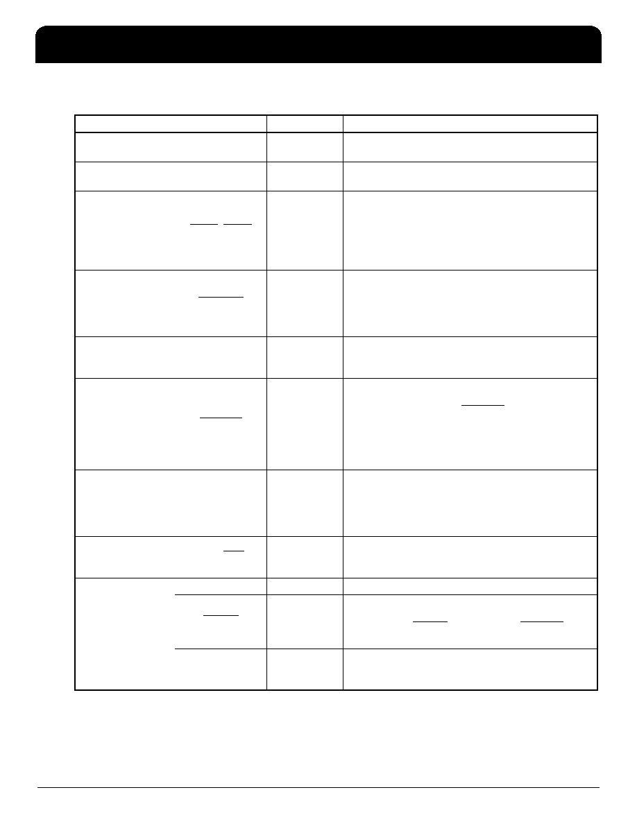
Ball Assignment
Signal Group
Signal Name
Type
Description
Ungated Inputs
DCKE0, DCKE1,
DODT0, DODT1
SSTL_18
DRAM function pins not associated with Chip Select.
Chip Select Gated
Inputs
D0 ... D21
SSTL_18
DRAM inputs, re-driven only when Chip Select is
LOW.
Chip Select Inputs
DCS0, DCS1
SSTL_18
DRAM Chip Select signals. These pins initiate DRAM
address/command decodes, and as such at least one
will be low when a valid address/command is present.
The register can be programmed to re-drive all
D-inputs only (CSGateEN high) when at least one
Chip Select input is LOW.
Re-Driven
Q0A...Q21A,
Q0B...Q21B,
QCSnA,B
QCKEnA,B,
QODTnA,B
SSTL_18
Outputs of the register, valid after the specified clock
count outputs and immediately following a rising edge
of the clock.
Parity Input
PARIN
SSTL_18
Input parity is received on pin PARIN and should
maintain odd parity across the D0...D21 inputs, at the
rising edge of the clock.
Parity Error
PTYERR
Open Drain
When LOW, this output indicates that a parity error
was output identified associated with the address
and/or command inputs. PTYERR will be active for
two clock cycles, and delayed by an additional clock
cycle for compatibility with final parity out timing on
the industry-standard DDR-II register with parity (in
JEDEC definition).
Program Inputs
CSGateEN
1.8V LVCMOS
Chip Select Gate Enable. When HIGH, the D0..D21
inputs will be latched only when at least one Chip
Select input is LOW during the rising edge of the
clock. When LOW, the D0...D21 inputs will be latched
and redriven on every rising edge of the clock.
Clock Inputs
CLK, CLK
SSTL_18
Differential master clock input pair to the register. The
register operation is triggered by a rising edge on the
positive clock input (CLK).
Miscellaneous
Inputs
MCL, MCH
Must be connected to a logic LOW or HIGH.
RESET
SSTL_18
Asynchronous reset input. When LOW, it causes a
reset of the internal latches, thereby forcing the
outputs LOW. RESET also resets the PTYERR
signal.
VREF
0.9V nominal
Input reference voltage for the SSTL_18 inputs. Two
pins (internally tied together) are used for increased
reliability.
相关PDF资料 |
PDF描述 |
|---|---|
| VE-B4M-IV-B1 | CONVERTER MOD DC/DC 10V 150W |
| VE-B4L-IV-B1 | CONVERTER MOD DC/DC 28V 150W |
| VE-JWK-MX-F3 | CONVERTER MOD DC/DC 40V 75W |
| MS3101A28-51S | CONN RCPT 12POS FREE HNG W/SCKT |
| VE-JWK-MX-F1 | CONVERTER MOD DC/DC 40V 75W |
相关代理商/技术参数 |
参数描述 |
|---|---|
| IDT74SSTUBF32865ABK8 | 功能描述:IC BUFFER 28BIT 1:2 REG 160-BGA RoHS:否 类别:集成电路 (IC) >> 逻辑 - 专用逻辑 系列:- 产品变化通告:Product Discontinuation 25/Apr/2012 标准包装:1,500 系列:74SSTV 逻辑类型:DDR 的寄存缓冲器 电源电压:2.3 V ~ 2.7 V 位数:14 工作温度:0°C ~ 70°C 安装类型:表面贴装 封装/外壳:48-TFSOP(0.240",6.10mm 宽) 供应商设备封装:48-TSSOP 包装:带卷 (TR) |
| IDT74SSTUBF32865ABKG | 功能描述:IC BUFFER 28BIT 1:2 REG 160-BGA RoHS:是 类别:集成电路 (IC) >> 逻辑 - 专用逻辑 系列:- 产品变化通告:Product Discontinuation 25/Apr/2012 标准包装:1,500 系列:74SSTV 逻辑类型:DDR 的寄存缓冲器 电源电压:2.3 V ~ 2.7 V 位数:14 工作温度:0°C ~ 70°C 安装类型:表面贴装 封装/外壳:48-TFSOP(0.240",6.10mm 宽) 供应商设备封装:48-TSSOP 包装:带卷 (TR) |
| IDT74SSTUBF32865ABKG8 | 功能描述:IC BUFFER 28BIT 1:2 REG 160-BGA RoHS:是 类别:集成电路 (IC) >> 逻辑 - 专用逻辑 系列:- 产品变化通告:Product Discontinuation 25/Apr/2012 标准包装:1,500 系列:74SSTV 逻辑类型:DDR 的寄存缓冲器 电源电压:2.3 V ~ 2.7 V 位数:14 工作温度:0°C ~ 70°C 安装类型:表面贴装 封装/外壳:48-TFSOP(0.240",6.10mm 宽) 供应商设备封装:48-TSSOP 包装:带卷 (TR) |
| IDT74SSTUBF32866BBFG | 功能描述:IC BUFFER 25BIT REG DDR2 96-BGA RoHS:是 类别:集成电路 (IC) >> 逻辑 - 专用逻辑 系列:- 产品变化通告:Product Discontinuation 25/Apr/2012 标准包装:1,500 系列:74SSTV 逻辑类型:DDR 的寄存缓冲器 电源电压:2.3 V ~ 2.7 V 位数:14 工作温度:0°C ~ 70°C 安装类型:表面贴装 封装/外壳:48-TFSOP(0.240",6.10mm 宽) 供应商设备封装:48-TSSOP 包装:带卷 (TR) |
| IDT74SSTUBF32866BBFG8 | 功能描述:IC BUFFER 25BIT CONF DDR2 96BGA RoHS:是 类别:集成电路 (IC) >> 逻辑 - 专用逻辑 系列:- 产品变化通告:Product Discontinuation 25/Apr/2012 标准包装:1,500 系列:74SSTV 逻辑类型:DDR 的寄存缓冲器 电源电压:2.3 V ~ 2.7 V 位数:14 工作温度:0°C ~ 70°C 安装类型:表面贴装 封装/外壳:48-TFSOP(0.240",6.10mm 宽) 供应商设备封装:48-TSSOP 包装:带卷 (TR) |
发布紧急采购,3分钟左右您将得到回复。