- 您现在的位置:买卖IC网 > PDF目录2000 > IDTNW6006AS (IDT, Integrated Device Technology Inc)IC CALLER ID DECODER 20-SOIC PDF资料下载
参数资料
| 型号: | IDTNW6006AS |
| 厂商: | IDT, Integrated Device Technology Inc |
| 文件页数: | 12/22页 |
| 文件大小: | 0K |
| 描述: | IC CALLER ID DECODER 20-SOIC |
| 标准包装: | 37 |
| 类型: | 来电身份解码器 |
| 应用: | 传真,调制解调器,寻呼机 |
| 电压 - 电源,模拟: | 2.5 V ~ 3.8 V |
| 电压 - 电源,数字: | 2.5 V ~ 3.8 V |
| 安装类型: | 表面贴装 |
| 封装/外壳: | 20-SOIC(0.295",7.50mm 宽) |
| 供应商设备封装: | 20-SOIC |
| 包装: | 管件 |
| 其它名称: | NW6006AS |
2
INDUSTRIAL TEMPERATURE RANGE
NW6006 ENHANCED TYPE II CALLER ID DECODER
WITH STUTTER DIAL TONE DETECTOR
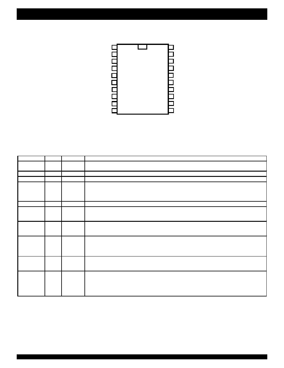
PIN INFORMATION
Figure 2. Pin Assignment
VREF
IN1+
IN1-
GS1
GND
OSCIN
OSCOUT
CB0
DCLK
DATA
IN2+
IN2-
GS2
CB2
CB1
VCC
CD/STRDT
ST/GT
EST
DR/STD
20
19
18
17
16
15
14
13
12
11
1
2
3
4
5
6
7
8
9
10
Name
Type
Pin No.
Description
VREF
O
1
Reference Voltage.
This output is used to bias the input OP amp. It is typically VCC/2.
IN1+
I
2
Non-inverting Input of the gain adjustable Tip/Ring OP amp.
IN1-
I
3
Inverting Input of the gain adjustable Tip/Ring OP amp.
GS1
O
4
Gain Select Output of the gain adjustable Tip/Ring OP amp.
The Tip/Ring signal can be attenuated or amplified at GS1 by adjusting the feedback resistor between GS1 and IN1-.
The FSK signal is always detected by Tip/Ring OP amp while DT-AS(CAS) signal can be detected by either Tip/Ring
or Hybrid OP amp. The OP amp selection is controlled by CB1 and CB2 bits.
GND
-
5
Ground.
OSCIN
I
6
Oscillator Input.
A 3.579545 MHz crystal or ceramic resonator should be connected between this pin and the OSCOUT. It can also
be driven by an external clock source.
OSCOUT
O
7
Oscillator Output.
A 3.579545 MHz crystal or ceramic resonator should be connected between this pin and the OSCIN. When an
external clock drives OSCIN, this pin can be left floating.
CB0
I
8
Control Bit 0 (FSK Data Interface Mode Select).
This pin can select the 3-wire FSK data interface mode. A ‘0’ on this pin indicates interface mode 0; while a ‘1’ on
this pin indicates interface mode 1. (The FSK data interface is consisted of DATA, DCLK and DR/STD pins.)
When CB0 is high and CB1, CB2 are both low, the device is set into the power down state.
DCLK
I/NC
9
Data Clock of the Serial FSK Interface.
In mode 0 (CB0 is low), this pin is unused; In mode 1 (CB0 is high), this pin is an input which clock the FSK data
byte out to the DATA pin.
DATA
O
10
Data Output of the Serial FSK Interface.
In mode 0 (CB0 is low), the FSK serial bit stream is output to the DATA pin directly.
In mode 1 (CB0 is high), the start bit is stripped off, the data byte and the stop bit is stored in a 9-bit buffer. At the
end of each word signaled by the DR/STD pin, the microcontroller should shift the byte out onto the DATA pin by
applying 8 read pulses to the DCLK pin. A 9th DCLK pulse will shift out the stop bit for framing error checking.
相关PDF资料 |
PDF描述 |
|---|---|
| IDTSSTE32882HLBBKG | IC REGISTERING CLK DRIVER 176BGA |
| IDTSSTE32882KA1AKG | IC REGISTERING CLK DRIVER 176BGA |
| ISD1750SYR | IC VOICE REC/PLAY 50SEC 28-SOIC |
| ISD5008EYI | IC VOICE REC/PLAY 4-8MIN 28-TSOP |
| ISL12008IB8Z | IC RTC I2C LO-POWER 8-SOIC |
相关代理商/技术参数 |
参数描述 |
|---|---|
| IDTP62000NLG | 制造商:Integrated Device Technology Inc 功能描述:IC PWM CTRLR 2/3/4-PHASE 64QFN |
| IDTP62000NLG8 | 制造商:Integrated Device Technology Inc 功能描述:IC PWM CTRLR 2/3/4-PHASE 64QFN |
| IDTP63131-00NDGI | 制造商:Integrated Device Technology Inc 功能描述:IC BUCK CTRLR MULTI-PH 40QFN |
| IDTP63131-00NDGI8 | 制造商:Integrated Device Technology Inc 功能描述:IC BUCK CTRLR MULTI-PH 40QFN |
| IDTP63133-00NDGI | 制造商:Integrated Device Technology Inc 功能描述:IC BUCK CTRLR MULTI-PH 40QFN |
发布紧急采购,3分钟左右您将得到回复。