- 您现在的位置:买卖IC网 > PDF目录61094 > IL300-DEFG (VISHAY INTERTECHNOLOGY INC) SPECIALTY OPTOELECTRONIC DEVICE PDF资料下载
参数资料
| 型号: | IL300-DEFG |
| 厂商: | VISHAY INTERTECHNOLOGY INC |
| 元件分类: | 光电元器件 |
| 英文描述: | SPECIALTY OPTOELECTRONIC DEVICE |
| 文件页数: | 6/8页 |
| 文件大小: | 444K |
| 代理商: | IL300-DEFG |
Document Number: 83622
www.vishay.com
Revision 17-August-01
6
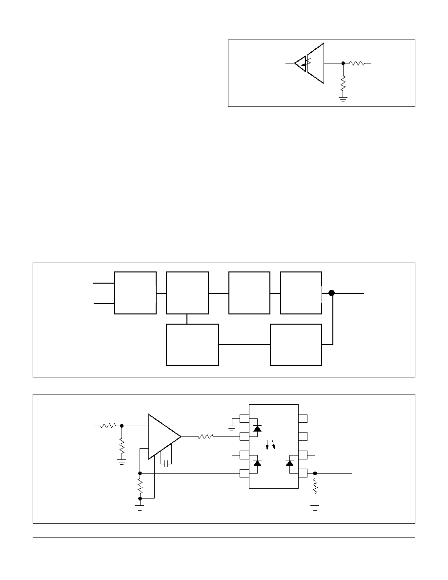
Figure 16. Isolated control amplier
For best input offset compensation at U1, R2 will equal R3. The
value of R1 can easily be calculated from the following.
The value of R5 depends upon the IL300 Transfer Gain (K3). K3
is targeted to be a unit gain device, however to minimize the
part to part Transfer Gain variation, Inneon offers K3 graded
into
% bins. R5 can determined using the following equation,
Or if a unity gain amplier is being designed
(VMONITOR=VOUT, R1=0), the equation simplies to:
+
-
Voltage
Monitor
R1
R2
To Control
Input
ISO
AMP
+1
R1
R2
V
MONITOR
V
a
---------------------------
1
–
=
5
±
R5
V
OUT
V
MONITOR
---------------------------
R3 R1
R2
+
()
R2K3
-----------------------------------
=
R5
R3
K3
-------
=
The isolated amplier provides the PWM control signal which is
derived from the output supply voltage. Figure 16 more closely
shows the basic function of the amplier.
The control amplier consists of a voltage divider and a non-
inverting unity gain stage. The TDA4918 data sheet indicates
that an input to the control amplier is a high quality opera-
tional amplier that typically requires a +3.0 V signal. Given
this information, the amplier circuit topology shown in Figure
18 is selected.
The power supply voltage is scaled by R1 and R2 so that there
is +3.0 V at the non-inverting input (Va) of U1. This voltage is
offset by the voltage developed by photocurrent owing
through R3. This photocurrent is developed by the optical ux
created by current owing through the LED. Thus as the scaled
monitor voltage (Va) varies it will cause a change in the LED
current necessary to satisfy the differential voltage needed
across R3 at the inverting input.
The rst step in the design procedure is to select the value of
R3 given the LED quiescent current (IFq) and the servo gain
(K1). For this design, IFq=12 mA. Figure 4 shows the servo
photocurrent at IFq is found to be 100 A. With this data R3 can
be calculated.
R3
V
b
I
Pl
------
3V
100
A
------------------
=
30K
=
Figure 17. Switch mode power supply
Figure 18. DC coupled power supply feedback amplier
SWITCH
XFORMER
SWITCH
MODE
REGULATOR
TDA4918
ISOLATED
FEEDBACK
CONTROL
110/
220
MAIN
DC OUTPUT
AC/DC
RECTIFIER
AC/DC
RECTIFIER
8
7
6
5
100 pF
4
3
1
2
8
6
7
K1
V
CC
V
CC
1
2
3
4
K2
V
CC
Vmonitor
R1
20 K
R2
30 K
R3
30 K
R4
100
Vout
To
control
input
R5
30 K
IL300
Vb
Va
+
-
U1
LM201
相关PDF资料 |
PDF描述 |
|---|---|
| IL300-F-X001 | SPECIALTY OPTOELECTRONIC DEVICE |
| IL300-X001 | SPECIALTY OPTOELECTRONIC DEVICE |
| IL300-X001 | SPECIALTY OPTOELECTRONIC DEVICE |
| IL300-X007T | SPECIALTY OPTOELECTRONIC DEVICE |
| IL300-X009T | SPECIALTY OPTOELECTRONIC DEVICE |
相关代理商/技术参数 |
参数描述 |
|---|---|
| IL300-DEFG-X001 | 功能描述:高线性光耦合器 High Gain Wide Bandwidth Linear RoHS:否 制造商:Avago Technologies 输入类型:AC/DC 最大正向二极管电压:1.95 V 最大反向二极管电压:2.5 V 最大输入二极管电流:25 mA 最大功率耗散:60 mW 最大工作温度:+ 100 C 最小工作温度:- 55 C 封装 / 箱体:DIP-8 Gull Wing 封装:Tube |
| IL300-DEFG-X006 | 功能描述:高线性光耦合器 Single Linear, High Gain, Wide Bandwidth RoHS:否 制造商:Avago Technologies 输入类型:AC/DC 最大正向二极管电压:1.95 V 最大反向二极管电压:2.5 V 最大输入二极管电流:25 mA 最大功率耗散:60 mW 最大工作温度:+ 100 C 最小工作温度:- 55 C 封装 / 箱体:DIP-8 Gull Wing 封装:Tube |
| IL300-DEFG-X007 | 功能描述:高线性光耦合器 High Gain Wide Bandwidth Linear RoHS:否 制造商:Avago Technologies 输入类型:AC/DC 最大正向二极管电压:1.95 V 最大反向二极管电压:2.5 V 最大输入二极管电流:25 mA 最大功率耗散:60 mW 最大工作温度:+ 100 C 最小工作温度:- 55 C 封装 / 箱体:DIP-8 Gull Wing 封装:Tube |
| IL300-DEFG-X007 | 制造商:Vishay Semiconductors 功能描述:; Leaded Process Compatible:Yes; Peak Re |
| IL300-DEFG-X007T | 功能描述:高线性光耦合器 Single Linear, High Gain, Wide Bandwidth RoHS:否 制造商:Avago Technologies 输入类型:AC/DC 最大正向二极管电压:1.95 V 最大反向二极管电压:2.5 V 最大输入二极管电流:25 mA 最大功率耗散:60 mW 最大工作温度:+ 100 C 最小工作温度:- 55 C 封装 / 箱体:DIP-8 Gull Wing 封装:Tube |
发布紧急采购,3分钟左右您将得到回复。