- 您现在的位置:买卖IC网 > PDF目录67720 > IMISC643AYB PROC SPECIFIC CLOCK GENERATOR, PDSO48 PDF资料下载
参数资料
| 型号: | IMISC643AYB |
| 元件分类: | 时钟产生/分配 |
| 英文描述: | PROC SPECIFIC CLOCK GENERATOR, PDSO48 |
| 封装: | SSOP-48 |
| 文件页数: | 7/12页 |
| 文件大小: | 138K |
| 代理商: | IMISC643AYB |
SC643
I
2C Clock Generator for 3 DIMM, Pentium
II Designs
Approved Product
INTERNATIONAL MICROCIRCUITS, INC. 525 LOS COCHES ST.
Rev.1.6
6/20/97
MILPITAS, CA 95035. TEL: 408-263-6300. FAX 408-263-6571
Page 4 of 12
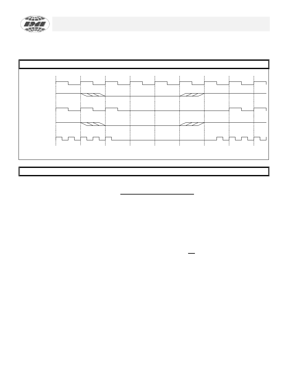
POWER MANAGEMENT TIMING
PCICLK_F
PCI_STOP#
PCICLK(0:5)
CPU_STOP#
CPUCLK(0:3)
Fig. 2
2-WIRE I
2C CONTROL INTERFACE
The 2-wire control interface implements a write only slave interface. The IMISC643 cannot be read back.
Sub-addressing is not supported, thus all preceeding bytes must be sent in order to change one of the
control bytes. The 2-wire control interface allows each clock output to be individually enabled or disabled.
During normal data transfer, the SDATA signal only changes when the SDCLK signal is low, and is stable
when SDCLK is high. There are two exceptions to this. A high to low transition on SDATA while SDCLK is
high is used to indicate the start of a data transfer cycle. A low to high transition on SDATA while SDCLK is
high indicates the end of a data transfer cycle. Data is always sent as complete 8-bit bytes, after which an
acknowledge is generated. The first byte of a transfer cycle is a 7-bit address with a Read/Write bit as the
LSB. Data is transferred MSB first.
The IMISC643 will respond to writes to 10 bytes (max) of data to address D2 by generating the acknowledge
(low) signal on the SDATA wire following reception of each byte.
The IMISC643 will not respond to any
other control interface conditions. Previously set control registers are retained.
相关PDF资料 |
PDF描述 |
|---|---|
| IMISC670DYB | PROC SPECIFIC CLOCK GENERATOR, PDSO48 |
| IMISG522BXB | OTHER CLOCK GENERATOR, PDSO16 |
| IMISG522BX | 120 MHz, OTHER CLOCK GENERATOR, PDSO16 |
| IMISG524BX | 120 MHz, OTHER CLOCK GENERATOR, PDSO16 |
| IMISG570CYB | PROC SPECIFIC CLOCK GENERATOR, PDSO48 |
相关代理商/技术参数 |
参数描述 |
|---|---|
| IMISC652EYB | 制造商:未知厂家 制造商全称:未知厂家 功能描述:CPU System Clock Generator |
| IMISC660 | 制造商:未知厂家 制造商全称:未知厂家 功能描述:Clocks and Buffers |
| IMISC660EYB | 制造商:International Microcircuits Inc 功能描述:LOW SKEW CLOCK DRIVER, PDSO28 |
| IMISC670DYB | 制造商:未知厂家 制造商全称:未知厂家 功能描述:CPU System Clock Generator |
| IMISC671CTB | 制造商:未知厂家 制造商全称:未知厂家 功能描述:CPU System Clock Generator |
发布紧急采购,3分钟左右您将得到回复。