- 您现在的位置:买卖IC网 > PDF目录67720 > IMISG570CYB (CYPRESS SEMICONDUCTOR CORP) PROC SPECIFIC CLOCK GENERATOR, PDSO48 PDF资料下载
参数资料
| 型号: | IMISG570CYB |
| 厂商: | CYPRESS SEMICONDUCTOR CORP |
| 元件分类: | 时钟产生/分配 |
| 英文描述: | PROC SPECIFIC CLOCK GENERATOR, PDSO48 |
| 封装: | SSOP-48 |
| 文件页数: | 4/14页 |
| 文件大小: | 176K |
| 代理商: | IMISG570CYB |
SG570
I
2C Frequency Clock Generator w/ EMI Reduction Spread Spectrum Technology
for Pentium Processor Based Designs.
Preliminary
INTERNATIONAL MICROCIRCUITS, INC. 525 LOS COCHES ST.
Rev.1.1
3/23/98
MILPITAS, CA 95035. TEL: 408-263-6300. FAX 408-263-6571
Page 12 of 14
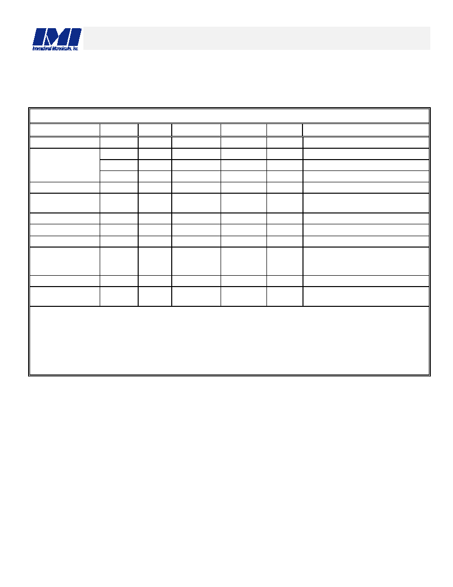
CRYSTAL AND REFERENCE OSCILLATOR PARAMETERS
Characteristic
Symbol
Min
Typ
Max
Units
Conditions
Frequency
Fo
12.00
14.31818
16.00
MHz
Tolerence
TC
-
+/-100
PPM
Calibration note 1
TS
-
+/- 100
PPM
Stability (Ta -10 to +60C) note 1
TA
-
5
PPM
Aging (first year @ 25C) note 1
Mode
OM
-
Parallell Resonant
Pin Capacitance
CP
6
pF
Capacitance of XIN and Xout pins
to ground (each)
DC Bias Voltage
VBIAS
0.3Vdd
Vdd/2
0.7Vdd
V
Startup time
Ts
-
30
S
Load Capacitance
CL
-
20
-
pF
the crystals rated load. note 1
Effective Series
resonant
resistance
R1
-
40
Ohms
Power Dissipation
DL
-
0.10
mW
note 1
Shunt Capacitance
CO
-
--
8
pF
crystals internal package
capacitance (total)
For maximum accuracy,the total circuit loading capacitance should be equal to CL. This loading capacitance is the
effective capacitance across the crystal pins and includes the device pin capacitance (CP) in parallel with any circuit
traces, the clock generator and any onboard discrete load capacitors.
Budgeting Calculations
Typical trace capacitance, (< half inch) is 4 pF, Load to the crystal is therefore
2.0 pF
Clock generator internal pin capacitance of 36 pF, Load to the crystal is therefore
3.0 pF
External crystal loading capacitors (connect to ground)
15.0 pF
the total parasitic capacitance would therefore be
= 20.0.0 pF.
Note 1: It is recommended but not mandatory that a crystal meets these specifications.
相关PDF资料 |
PDF描述 |
|---|---|
| IMISG570CYB | PROC SPECIFIC CLOCK GENERATOR, PDSO48 |
| IMISM532AXB | OTHER CLOCK GENERATOR, PDSO16 |
| IMSA113-J20S | ACTIVE DELAY LINE, PQCC44 |
| IMSB419-4 | SPECIALTY MICROPROCESSOR CIRCUIT, XMA16 |
| IMSC011-E20S | 1 CHANNEL(S), 20M bps, SERIAL COMM CONTROLLER, PDSO28 |
相关代理商/技术参数 |
参数描述 |
|---|---|
| IMISG571DTB | 制造商:未知厂家 制造商全称:未知厂家 功能描述:CPU System Clock Generator |
| IMISG571DYB | 制造商:未知厂家 制造商全称:未知厂家 功能描述:CPU System Clock Generator |
| IMISG577CYB | 制造商:未知厂家 制造商全称:未知厂家 功能描述:CPU System Clock Generator |
| IMISG745BYB | 制造商:未知厂家 制造商全称:未知厂家 功能描述:CPU System Clock Generator |
| IMISG748CYB | 制造商:未知厂家 制造商全称:未知厂家 功能描述:CPU System Clock Generator |
发布紧急采购,3分钟左右您将得到回复。