- 您现在的位置:买卖IC网 > PDF目录13423 > IP1201PBF (International Rectifier)IC REG BUCK SYNC ADJ 30A 198BGA PDF资料下载
参数资料
| 型号: | IP1201PBF |
| 厂商: | International Rectifier |
| 文件页数: | 20/29页 |
| 文件大小: | 0K |
| 描述: | IC REG BUCK SYNC ADJ 30A 198BGA |
| 产品变化通告: | (EP) Parts Discontinuation 25/May/2012 |
| 标准包装: | 10 |
| 系列: | iPOWIR™ |
| 类型: | 降压(降压) |
| 输出类型: | 可调式 |
| 输出数: | 2 |
| 输出电压: | 0.8 V ~ 3.3 V |
| 输入电压: | 3.14 V ~ 5.5 V |
| PWM 型: | 电流模式 |
| 频率 - 开关: | 200kHz ~ 400kHz |
| 电流 - 输出: | 30A |
| 同步整流器: | 是 |
| 工作温度: | -40°C ~ 125°C |
| 安装类型: | 表面贴装 |
| 封装/外壳: | 198-BGA(159 凸块) |
| 包装: | 散装 |
| 供应商设备封装: | BGA(15.5x9.25) |
| 配用: | IRDCIP1201-A-ND - BUCK CONV REF DESIGN KIT IP1201 |
第1页第2页第3页第4页第5页第6页第7页第8页第9页第10页第11页第12页第13页第14页第15页第16页第17页第18页第19页当前第20页第21页第22页第23页第24页第25页第26页第27页第28页第29页
�� �
�
�iP1201PbF�
�3.� Place� a� zero� at� 75%� of� f� LC� to� cancel� one� of� the� LC�
�filter� poles.�
�Vout1�
�R26�
�C22�
�C9�
�f� z� =� 0� .� 75� �
�2� π�
�1�
�L� o� � C� o�
�(13)�
�C21�
�CC1�
�4.� Calculate� C� 9� using� equations� (11)� and� (13)�
�R25�
�R9�
�iP1201PbF�
�FB1�
�Calculation� of� compensation� components� for� out-�
�put1,� based� on� the� example� above� yields:�
�f� LC� =� 4.0kHz�
�f� z� =� 3.0kHz�
�f� 0� =� 20kHz� (based� on� F� sw� =� 200kHz)�
�f� esr� =� 10kHz,� per� equation� (7)� using� R� esr� =� 11m� ?� .�
�R� 5� =� 4.5K�
�C� 9� =� 12nF�
�R7�
�C10�
�Magnitude(dB)�
�H(s)� dB�
�VREF�
�E/A1�
�The� same� steps� can� be� used� to� determine� the� val-�
�ues� of� the� compensation� components� for� output2.�
�FZ1�
�FZ2�
�FP2�
�FP3�
�Frequency�
�f� p� 2� ≈�
�2� π� ×� R� 5� ×� C� opt�
�C� opt� =�
�1�
�2� π� ×� f� p� 2� ×� R� 5�
�f� z� =�
�2� π� ×� R� 25� ×� C� 21�
�f� p� 3� ?�
�(19)�
�f� z� 1� =�
�(20)�
�1�
�f� z� 2�
�(22)�
�f� 0� =�
�� V� IN� � R� 26� � C� 21� �
�Sometimes, a pole f� p2� is added at half the switching�
�frequency� to� filter� the� switching� noise.� This� is� done�
�by� adding� a� capacitor� C� opt� in� Fig.20� from� the� output� of�
�the� error� amplifier� (CC� pin� of� iP1201PbF)� to� ground.�
�This� pole� is� given� by� equation� (14):�
�1�
�(14)�
�C� opt� is� found� from� equation� (15)� by� rearranging� the� terms�
�in� equation� (14)� and� by� setting� f� p2� =� f� sw� /� 2:�
�(15)�
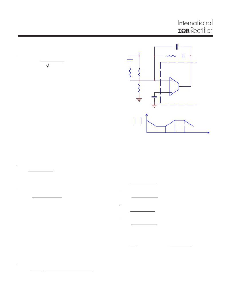
�Type� III�
�Type� III� compensation� scheme� allows� the� use� of� any�
�type� of� capacitors� with� esr� frequency� of� any� range.� This�
�scheme� suggests� a� double� pole� double� zero� compen-�
�sation� and� requires� more� components� around� the� er-�
�ror� amplifier� to� achieve� the� desired� gain� and� phase�
�margins.� Fig.� 21� represents� the� type� III� compensation�
�network� for� iP1201PbF.�
�The� transfer� function� of� the� type� III� compensator� is�
�given� by� eqaution� (16)�
�Fig.� 21:� Typical� Type� III� compensation� and� its� gain�
�plot�
�The� frequencies� of� the� three� poles� and� the� two� zeros�
�of� the� type� III� compensation� scheme� are� represented�
�by� the� following� equations:�
�f� p1� =� 0� (17)�
�1�
�(18)�
�1�
�2� π� ×� R� 2� 6� ×� C� 22�
�1�
�2� π� ×� R� 26� ×� C� 9�
�=� (21)�
�2� π� ×� R� 9� ×� C� 21�
�The� crossover� frequency� f� 0� for� type� III� compensation� is�
�represented� by� equation� (22):�
�1� 1�
�V� ramp� 2� π� ×� L� 0� ×� C� 0�
�Follow� the� steps� below� to� determine� the� feedback� loop�
�compensation� component� values:�
�H� (� s� )� ≈�
�20�
�1�
�sR� 9� C� 9�
��
�(� 1� +� sR� 26� C� 9� )� � (� 1� +� sR� 9� C� 21� )�
�(� 1� +� sR� 26� C� 22� )� � (� 1� +� sR� 25� C� 21� )�
�(16)�
�1.� Select� a� zero� db� crossover� frequency� f� 0� in� the� range�
�of� 10%� to� 20%� of� the� switching� frequency� f� sw.�
�www.irf.com�
�相关PDF资料 |
PDF描述 |
|---|---|
| MAX8214BCSE+T | IC MONITOR VOLT MPU 16-SOIC |
| IP1202PBF | IC REG BUCK SYNC ADJ 30A 198BG |
| MAX8213BCSE+T | IC MONITOR VOLT MPU 16-SOIC |
| RBM40DTMD-S189 | CONN EDGECARD 80POS R/A .156 SLD |
| GCM36DTBD-S664 | CONN EDGECARD 72POS R/A .156 |
相关代理商/技术参数 |
参数描述 |
|---|---|
| IP1201TR | 功能描述:开关变换器、稳压器与控制器 DUAL OUTPUT 2-Phase 3.14 to 5V 400kHz RoHS:否 制造商:Texas Instruments 输出电压:1.2 V to 10 V 输出电流:300 mA 输出功率: 输入电压:3 V to 17 V 开关频率:1 MHz 工作温度范围: 安装风格:SMD/SMT 封装 / 箱体:WSON-8 封装:Reel |
| IP1201TRPBF | 功能描述:开关变换器、稳压器与控制器 DUAL OUTPUT 2-Phase 3.14 to 5V 400kHz RoHS:否 制造商:Texas Instruments 输出电压:1.2 V to 10 V 输出电流:300 mA 输出功率: 输入电压:3 V to 17 V 开关频率:1 MHz 工作温度范围: 安装风格:SMD/SMT 封装 / 箱体:WSON-8 封装:Reel |
| IP1202 | 功能描述:开关变换器、稳压器与控制器 DUAL OUTPUT 2-Phase 5.5V to 13.2V 15A RoHS:否 制造商:Texas Instruments 输出电压:1.2 V to 10 V 输出电流:300 mA 输出功率: 输入电压:3 V to 17 V 开关频率:1 MHz 工作温度范围: 安装风格:SMD/SMT 封装 / 箱体:WSON-8 封装:Reel |
| IP1202PBF | 功能描述:开关变换器、稳压器与控制器 DUAL OUTPUT 2-Phase 5.5V to 13.2V 15A RoHS:否 制造商:Texas Instruments 输出电压:1.2 V to 10 V 输出电流:300 mA 输出功率: 输入电压:3 V to 17 V 开关频率:1 MHz 工作温度范围: 安装风格:SMD/SMT 封装 / 箱体:WSON-8 封装:Reel |
| IP1202PBF-EL | 制造商:International Rectifier 功能描述: |
发布紧急采购,3分钟左右您将得到回复。